

VISHAY VS-30BQ100 Datasheet
www.vishay.com
Cathode Anode
SMC
High Performance Schottky Rectifier, 3 A
PRODUCT SUMMARY
Package SMC
I
F(AV)
V
R
V
at I
F
F
I
RM
T
max. 175 °C
J
Diode variation Single die
E
AS
3.0 A
100 V
0.62 V
5 mA at 125 °C
3.0 mJ
VS-30BQ100-M3
Vishay Semiconductors
FEATURES
• Low forward voltage drop
• Guard ring for enhanced ruggedness and long
term reliability
• Small foot print, surface mountable
• High frequency operation
• Meets MSL level 1, per J-STD-020, LF maximum peak of
260 °C
• Material categorization: for definitions of compliance
please see www.vishay.com/doc?99912
DESCRIPTION
The VS-30BQ100-M3 surface mount Schottky rectifier has
been designed for applications requiring low forward drop
and small foot prints on PC boards. Typical applications are
in disk drives, switching power supplies, converters,
freewheeling diodes, battery charging, and reverse battery
protection.
MAJOR RATINGS AND CHARACTERISTICS
SYMBOL CHARACTERISTICS VALUES UNITS
I
F(AV)
V
I
FSM
V
T
RRM
F
J
Rectangular waveform 3.0 A
100 V
tp = 5 μs sine 800 A
3.0 Apk, TJ = 125 °C 0.62 V
Range -55 to +175 °C
VOLTAGE RATINGS
PARAMETER SYMBOL VS-30BQ100-M3 UNITS
Maximum DC reverse voltage V
Maximum working peak reverse voltage V
R
RWM
100 V
ABSOLUTE MAXIMUM RATINGS
PARAMETER SYMBOL TEST CONDITIONS VALUES UNITS
Maximum average forward current I
Maximum peak one cycle
non-repetitive surge current
Non-repetitive avalanche energy E
Repetitive avalanche current I
F(AV)
I
FSM
AS
AR
50 % duty cycle at TL = 148 °C, rectangular waveform 3.0
50 % duty cycle at T
5 μs sine or 3 μs rect. pulse
10 ms sine or 6 ms rect. pulse 70
TJ = 25 °C, IAS = 1.0 A, L = 6 mH 3.0 mJ
Current decaying linearly to zero in 1 μs
Frequency limited by T
= 138 °C, rectangular waveform 4.0
L
Following any rated
load condition and with
rated V
maximum VA = 1.5 x VR typical
J
RRM
applied
800
0.5 A
A
Revision: 13-Sep-10
1
For technical questions within your region: DiodesAmericas@vishay.com
THIS DOCUMENT IS SUBJECT TO CHANGE WITHOUT NOTICE. THE PRODUCTS DESCRIBED HEREIN AND THIS DOCUMENT
ARE SUBJECT TO SPECIFIC DISCLAIMERS, SET FORTH AT www.vishay.com/doc?91000
, DiodesAsia@vishay.com, DiodesEurope@vishay.com
Document Number: 93360
VS-30BQ100-M3
dP
tot
dT
J
-------------
1
R
thJA
--------------<
www.vishay.com
ELECTRICAL SPECIFICATIONS
PARAMETER SYMBOL TEST CONDITIONS VALUES UNITS
3 A
Maximum forward voltage drop V
FM
(1)
3 A
6 A 0.90
6 A 0.70
Maximum reverse leakage current I
Maximum junction capacitance C
Typical series inductance L
RM
T
S
TJ = 25 °C
T
= 125 °C 5.0
J
VR = 5 VDC (test signal range 100 kHz to 1 MHz), 25 °C 115 pF
Measured lead to lead 5 mm from package body 3.0 nH
Maximum voltage rate of change dV/dt Rated V
R
T
= 25 °C
J
= 125 °C
T
J
V
= Rated V
R
Note
(1)
Pulse width = 300 μs, duty cycle = 2 %
THERMAL - MECHANICAL SPECIFICATIONS
PARAMETER SYMBOL TEST CONDITIONS VALUES UNITS
Maximum junction and
storage temperature range
Maximum thermal resistance,
junction to lead
Maximum thermal resistance,
junction to ambient
Approximate weight
Marking device Case style SMC (similar to DO-214AB) 3J
Notes
(1)
(2)
Mounted 1" square PCB
thermal runaway condition for a diode on its own heatsink
(1)
T
, T
J
Stg
(2)
R
thJL
DC operation
R
thJA
Vishay Semiconductors
0.79
0.62
0.5
R
10 000 V/μs
-55 to +175 °C
12
46
0.24 g
0.008 oz.
V
mA
°C/W
Revision: 13-Sep-10
For technical questions within your region: DiodesAmericas@vishay.com
THIS DOCUMENT IS SUBJECT TO CHANGE WITHOUT NOTICE. THE PRODUCTS DESCRIBED HEREIN AND THIS DOCUMENT
ARE SUBJECT TO SPECIFIC DISCLAIMERS, SET FORTH AT www.vishay.com/doc?91000
2
, DiodesAsia@vishay.com, DiodesEurope@vishay.com
Document Number: 93360
www.vishay.com
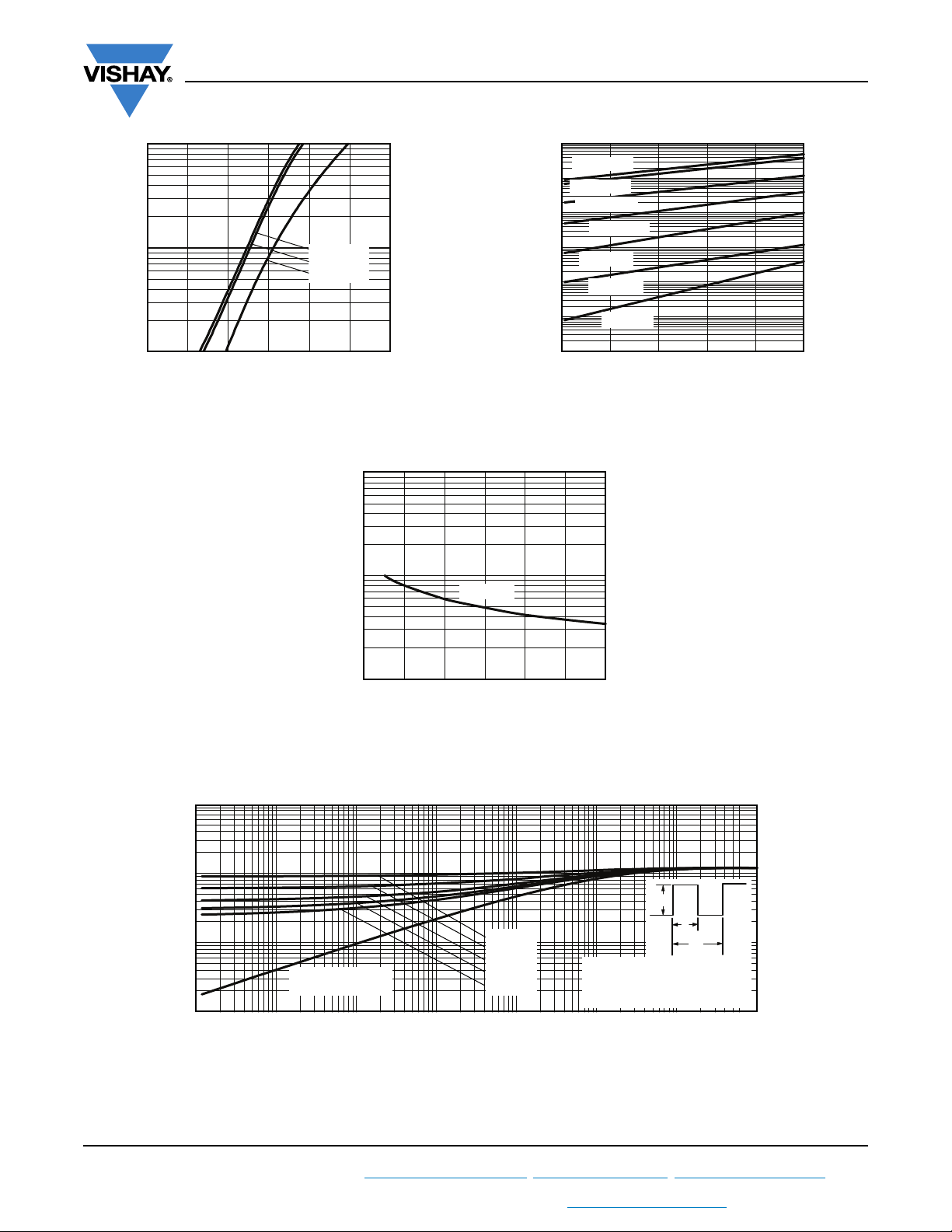
0.1
1
10
I
F
- Instantaneous Forward Current (A)
V
FM
- Forward Voltage Drop (V)
0.2 0.8 1.210.40 0.6
TJ = 175 °C
T
J
= 125 °C
T
J
= 25 °C
0.001
0.0001
0.00001
1
0.1
0.01
10
I
R
- Reverse Current (mA)
VR - Reverse Voltage (V)
20 40 60 800 100
TJ = 175 °C
T
J
= 125 °C
TJ = 100 °C
TJ = 50 °C
TJ = 75 °C
TJ = 25°C
TJ = 150 °C
10
100
1000
C
T
- Junction Capacitance (pF)
VR - Reverse Voltage (V)
20 40 600
TJ = 25 °C
VS-30BQ100-M3
Vishay Semiconductors
Fig. 1 - Maximum Forward Voltage Drop Characteristics (Per Leg) Fig. 2 - Typical Values of Reverse Current vs.
Reverse Voltage (Per Leg)
Fig. 3 - Typical Junction Capacitance vs. Reverse Voltage (Per Leg)
100
10
1
Revision: 13-Sep-10
- Thermal Impedance (°C/W)
thJC
Z
0.1
0.00001 0.0001 0.001 0.01 0.1
For technical questions within your region: DiodesAmericas@vishay.com
THIS DOCUMENT IS SUBJECT TO CHANGE WITHOUT NOTICE. THE PRODUCTS DESCRIBED HEREIN AND THIS DOCUMENT
P
DM
t
Single pulse
(thermal resistance)
D = 0.75
D = 0.50
D = 0.33
D = 0.25
D = 0.20
Notes:
1. Duty factor D = t
2. Peak TJ = PDM x Z
1 10010
1/t2
1
thJC
t
2
.
+ T
t1 - Rectangular Pulse Duration (s)
Fig. 4 - Maximum Thermal Impedance Z
Characteristics (Per Leg)
thJC
3
, DiodesAsia@vishay.com, DiodesEurope@vishay.com
ARE SUBJECT TO SPECIFIC DISCLAIMERS, SET FORTH AT www.vishay.com/doc?91000
C
Document Number: 93360
 Loading...