Vishay VS-20ETS08SPbF High Voltage Series, VS-20ETS12SPbF High Voltage Series Data Sheet

VS-20ETS08SPbF, VS-20ETS12SPbF High Voltage Series
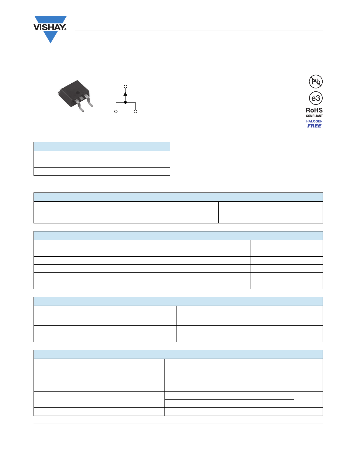
D2PAK
2
13
Base cathode
Anode Anode
PRODUCT SUMMARY
VF at 10 A < 1 V
I
FSM
V
RRM
Input Rectifier Diode, 20 A
FEATURES
• Meets MSL level 1, per J-STD-020, LF
maximum peak of 260 °C
• Compliant to RoHS directive 2002/95/EC
• Halogen-free according to IEC 61249-2-21
definition
• Designed and qualified for industrial level
APPLICATIONS
• Input rectification
• Vishay Semiconductors switches and output rectifiers
which are available in identical package outlines
300 A
800 V/1200 V
DESCRIPTION
The VS-20ETS...SPbF rectifier High Voltage Series has been
optimized for very low forward voltage drop, with moderate
leakage. The glass passivation technology used has reliable
operation up to 150 °C junction temperature.
Vishay Semiconductors
OUTPUT CURRENT IN TYPICAL APPLICATIONS
APPLICATIONS SINGLE-PHASE BRIDGE THREE-PHASE BRIDGE UNITS
Capacitive input filter T
common heatsink of 1 °C/W
= 55 °C, TJ = 125 °C
A
16.3 21 A
MAJOR RATINGS AND CHARACTERISTICS
SYMBOL CHARACTERISTICS VALUES UNITS
I
F(AV)
V
I
FSM
V
T
RRM
F
J
Sinusoidal waveform 20 A
800/1200 V
300 A
20 A, TJ = 25 °C 1.1 V
- 40 to 150 °C
VOLTAGE RATINGS
V
, MAXIMUM PEAK
PART NUMBER
VS-20ETS08SPbF 800 900
VS-20ETS12SPbF 1200 1300
RRM
REVERSE VOLTAGE
V
V
, MAXIMUM NON-REPETITIVE
RSM
PEAK REVERSE VOLTAGE
V
I
RRM
AT 150 °C
mA
1
ABSOLUTE MAXIMUM RATINGS
PARAMETER SYMBOL TEST CONDITIONS VALUES UNITS
Maximum average forward current I
Maximum peak one cycle
non-repetitive surge current
2
Maximum I
Maximum I
Document Number: 94340 For technical questions within your region, please contact one of the following: www.vishay.com
Revision: 28-Jul-10 DiodesAmericas@vishay.com
t for fusing I2t
2
t for fusing I2t t = 0.1 ms to 10 ms, no voltage reapplied 4420 A2s
F(AV)
I
FSM
TC = 105 °C, 180° conduction half sine wave 20
10 ms sine pulse, rated V
10 ms sine pulse, no voltage reapplied 300
10 ms sine pulse, rated V
10 ms sine pulse, no voltage reapplied 442
, DiodesAsia@vishay.com, DiodesEurope@vishay.com 1
applied 250
RRM
applied 316
RRM
A
2
A
s

VS-20ETS08SPbF, VS-20ETS12SPbF High Voltage Series
Vishay Semiconductors
Input Rectifier Diode, 20 A
ELECTRICAL SPECIFICATIONS
PARAMETER SYMBOL TEST CONDITIONS VALUES UNITS
Maximum forward voltage drop V
Forward slope resistance r
Threshold voltage V
Maximum reverse leakage current I
FM
F(TO)
RM
20 A, TJ = 25 °C 1.1 V
t
TJ = 150 °C
TJ = 25 °C
T
= 150 °C 1.0
J
V
= Rated V
R
RRM
10.4 m
0.85 V
0.1
THERMAL - MECHANICAL SPECIFICATIONS
PARAMETER SYMBOL TEST CONDITIONS VALUES UNITS
Maximum junction and storage temperature range T
Maximum thermal resistance,
junction to case
Maximum thermal resistance,
junction to ambient
Typical thermal resistance,
case to heatsink
, T
J
Stg
DC operation 1.3
R
thJC
(1)
R
thJA
R
thCS
For D2PAK version 62
Mounting surface, smooth and greased 0.5
Approximate weight
Mounting torque
Marking device Case style D
minimum 6.0 (5.0)
maximum 12 (10)
2
PAK (SMD-220)
Note
(1)
When mounted on 1” square (650 mm2) PCB of FR-4 or G-10 material 4 oz. (140 μm) copper 40 °C/W
For recommended footprint and soldering techniques refer to application note #AN-994
- 40 to 150 °C
2g
0.07 oz.
kgf · cm
(lbf · in)
20ETS08S
20ETS12S
mA
°C/W
www.vishay.com For technical questions within your region, please contact one of the following: Document Number: 94340
2 DiodesAmericas@vishay.com
, DiodesAsia@vishay.com, DiodesEurope@vishay.com Revision: 28-Jul-10

10
120
110
100
130
140
150
Maximum Allowable Case
Temperature (°C)
Average Forward Current (A)
46821012
20
22
14 16 18
0
30°
60°
90°
120°
180°
20ETS.. Series
R
thJC
(DC) = 1.3 °C/W
Conduction angle
Ø
90
140
150
130
120
110
100
Maximum Allowable Case
Temperature (°C)
Average Forward Current (A)
1051520
30
35
25
0
DC
30°
60°
90°
120°
180°
20ETS.. Series
R
thJC
(DC) = 1.3 °C/W
Ø
Conduction period
0
5
20
25
30
15
10
Maximum Average Forward
Power Loss (W)
Average Forward Current (A)
4
20
24
81216
0
RMS limit
180°
120°
90°
60°
30°
20ETS.. Series
T
J
= 150 °C
Conduction angle
Ø
50
300
250
200
150
100
Peak Half Sine Wave
Forward Current (A)
Number of Equal Amplitude Half
Cycle Current Pulse (N)
10
100
1
20ETS.. Series
At any rated load condition and with
rated V
RRM
applied following surge.
Initial T
J
= 150 °C
at 60 Hz 0.0083 s
at 50 Hz 0.0100 s
50
300
250
200
150
100
Peak Half Sine Wave
Forward Current (A)
Pulse Train Duration (s)
0.1
1
0.01
20ETS.. Series
Maximum non-repetitive surge current
versus pulse train duration.
Initial T
J
= 150 °C
No voltage reapplied
Rated V
RRM
reapplied
VS-20ETS08SPbF, VS-20ETS12SPbF High Voltage Series
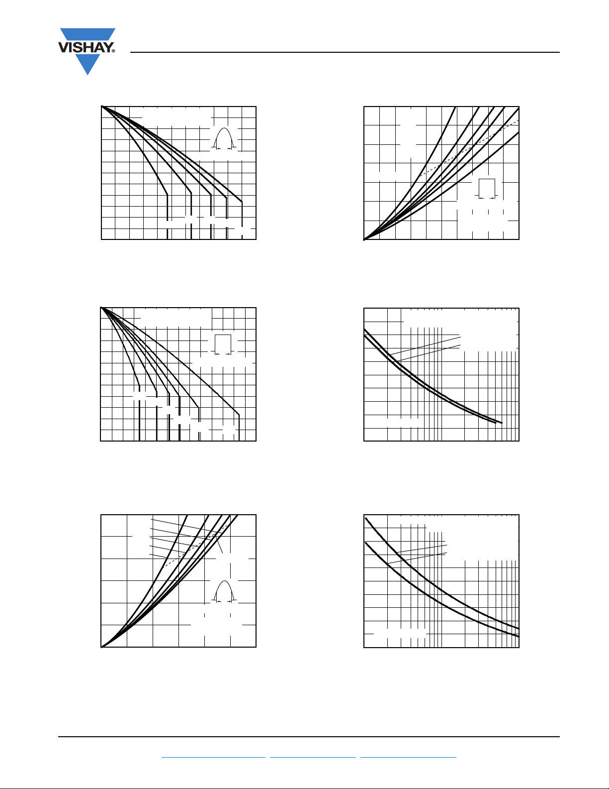
Fig. 1 - Current Rating Characteristics
Input Rectifier Diode, 20 A
35
30
25
20
15
Power Loss (W)
10
5
Maximum Average Forward
0
0
Fig. 4 - Forward Power Loss Characteristics
Vishay Semiconductors
DC
180°
120°
90°
60°
30°
RMS limit
Conduction period
20ETS.. Series
= 150 °C
T
J
51015
Average Forward Current (A)
Ø
20
25
Fig. 3 - Forward Power Loss Characteristics
Document Number: 94340 For technical questions within your region, please contact one of the following: www.vishay.com
Revision: 28-Jul-10 DiodesAmericas@vishay.com
Fig. 2 - Current Rating Characteristics
Fig. 5 - Maximum Non-Repetitive Surge Current
Fig. 6 - Maximum Non-Repetitive Surge Current
, DiodesAsia@vishay.com, DiodesEurope@vishay.com 3
 Loading...