Vishay VS-20ETF..SPbF Series Data Sheet

Base
common
cathode
+
3
Anode
2
1
Anode
--
VS-20ETF..SPbF Series
www.vishay.com
Vishay Semiconductors
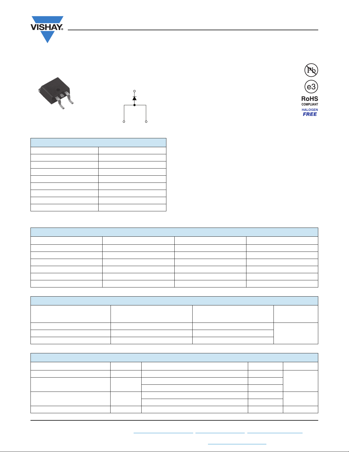
Surface Mountable Fast Soft Recovery Rectifier Diode, 20 A
FEATURES
• Meets MSL level 1, per J-STD-020, LF maximum
peak of 260 °C
• Designed and qualified according to
JEDEC-JESD47
• Compliant to RoHS Directive 2002/95/EC
• Halogen-free according to IEC 61249-2-21
definition
D2PAK (SMD-220)
PRODUCT SUMMARY
Package TO-263AB (D2PAK)
I
F(AV)
V
R
V
at I
F
F
I
FSM
t
rr
T
max. 150 °C
J
Diode variation Single die
Snap factor 0.6
20 A
200 V, 400 V, 600 V
1.3 V
300 A
60 ns
APPLICATIONS
• Output rectification and freewheeling in inverters,
choppers and converters
• Input rectifications where severe restrictions on
conducted EMI should be met
DESCRIPTION
The VS-20ETF..SPbF soft recovery rectifier series has been
optimized for combined short reverse recovery time and low
forward voltage drop.
The glass passivation ensures stable reliable operation in
the most severe temperature and power cycling conditions.
MAJOR RATINGS AND CHARACTERISTICS
SYMBOL CHARACTERISTICS VALUES UNITS
I
F(AV)
V
I
FSM
V
t
rr
T
RRM
F
J
Sinusoidal waveform 20 A
200 to 600 V
300 A
10 A, TJ = 25 °C 1.2 V
1 A, 100 A/μs 60 ns
Range - 40 to 150 °C
VOLTAGE RATINGS
, MAXIMUM PEAK
V
RRM
PART NUMBER
REVERSE VOLTAGE
V
VS-20ETF02SPbF 200 300
VS-20ETF06SPbF 600 700
V
, MAXIMUM NON-REPETITIVE
RSM
PEAK REVERSE VOLTAGE
V
AT 150 °C
ABSOLUTE MAXIMUM RATINGS
PARAMETER SYMBOL TEST CONDITIONS VALUES UNITS
Maximum average forward current I
Maximum peak one cycle
non-repetitive surge current
2
Maximum I
Maximum I
t for fusing I2t
2
t for fusing I2t t = 0.1 ms to 10 ms, no voltage reapplied 4420 A2s
F(AV)
I
FSM
Revision: 17-Aug-11
For technical questions within your region: DiodesAmericas@vishay.com
THIS DOCUMENT IS SUBJECT TO CHANGE WITHOUT NOTICE. THE PRODUCTS DESCRIBED HEREIN AND THIS DOCUMENT
ARE SUBJECT TO SPECIFIC DISCLAIMERS, SET FORTH AT www.vishay.com/doc?91000
TC = 97 °C, 180° conduction half sine wave 20
10 ms sine pulse, rated V
applied 250
RRM
10 ms sine pulse, no voltage reapplied 300
10 ms sine pulse, rated V
applied 316
RRM
10 ms sine pulse, no voltage reapplied 442
1
Document Number: 94097
, DiodesAsia@vishay.com, DiodesEurope@vishay.com
I
RRM
mA
5VS-20ETF04SPbF 400 500
A
2
s
A

I
FM
t
rr
dir
dt
I
RM(REC)
Q
rr
t
t
atb
VS-20ETF..SPbF Series
www.vishay.com
ELECTRICAL SPECIFICATIONS
PARAMETER SYMBOL TEST CONDITIONS VALUES UNITS
Maximum forward voltage drop V
Forward slope resistance r
Threshold voltage V
Maximum reverse leakage current I
FM
t
F(TO)
RM
20 A, TJ = 25 °C 1.30
60 A, T
= 25 °C 1.67
J
TJ = 150 °C 0.9 V
TJ = 25 °C
T
= 150 °C 5.0
J
V
= Rated V
R
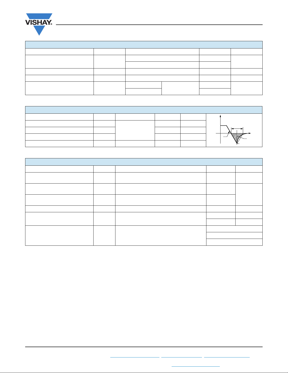
RECOVERY CHARACTERISTICS
PARAMETER SYMBOL TEST CONDITIONS VALUES UNITS
Reverse recovery time t
Reverse recovery current I
Reverse recovery charge Q
rr
rr
rr
IF at 20 Apk
100 A/μs
25 °C
Snap factor S Typical 0.6
160 ns
10 A
1.25 μC
Vishay Semiconductors
V
12.5 m
RRM
0.1
mA
THERMAL - MECHANICAL SPECIFICATIONS
PARAMETER SYMBOL TEST CONDITIONS VALUES UNITS
Maximum junction and storage
temperature range
Maximum thermal resistance,
junction to case
Maximum thermal resistance
junction to ambient (PCB mount)
Soldering temperature T
Approximate weight
Marking device Case style TO-263AB (D
Note
(1)
When mounted on 1" square (650 mm2) PCB of FR-4 or G-10 material 4 oz. (140 μm) copper 40 °C/W.
For recommended footprint and soldering techniques refer to application note #AN-994.
, T
T
J
Stg
R
DC operation 0.9
thJC
(1)
R
thJA
S
2
PAK)
- 40 to 150 °C
40
240 °C
2g
0.07 oz.
20ETF02S
20ETF04S
20ETF06S
°C/W
Revision: 17-Aug-11
For technical questions within your region: DiodesAmericas@vishay.com
THIS DOCUMENT IS SUBJECT TO CHANGE WITHOUT NOTICE. THE PRODUCTS DESCRIBED HEREIN AND THIS DOCUMENT
2
, DiodesAsia@vishay.com, DiodesEurope@vishay.com
ARE SUBJECT TO SPECIFIC DISCLAIMERS, SET FORTH AT www.vishay.com/doc?91000
Document Number: 94097

www.vishay.com
90
80
150
025
Maximum Allowable Case
Temperature (°C)
Average Forward Current (A)
15
530
110
35
120
100
10 20
130
140
20ETF.. Series
R
thJC
(DC) = 0.9 K/W
Ø
Conduction period
30°
60°
90°
120°
180°
DC
10
0
35
0
Maximum Average Forward
Power Loss (W)
Average Forward Current (A)
20
25
25
30
20
10 155
5
15
180°
120°
90°
60°
30°
RMS limit
20ETF.. Series
T
J
= 150 °C
Conduction angle
Ø
10
0
45
0
Maximum Average Forward
Power Loss (W)
Average Forward Current (A)
302535
35
15
10 205
15
25
20ETF.. Series
T
J
= 150 °C
Ø
Conduction period
RMS limit
180°
120°
90°
60°
30°
DC
5
20
30
40
450
150
50
0.001 0.01 1
Peak Half Sine Wave
Forward Current (A)
Pulse Train Duration (s)
300
100
200
250
350
550
Maximum non-repetitive surge current
versus pulse train duration.
20ETF.. Series
Initial TJ = 150 °C
No voltage reapplied
Rated V
RRM
reapplied
0.1
500
400
VS-20ETF..SPbF Series
Vishay Semiconductors
150
140
130
120
110
100
Temperature (°C)
90
Maximum Allowable Case
80
70
06
20ETF.. Series
(DC) = 0.9 K/W
R
thJC
Ø
Conduction angle
60°
30°
28
4
10 22
12 14
120° 180°
90°
16 18 20
Average Forward Current (A)
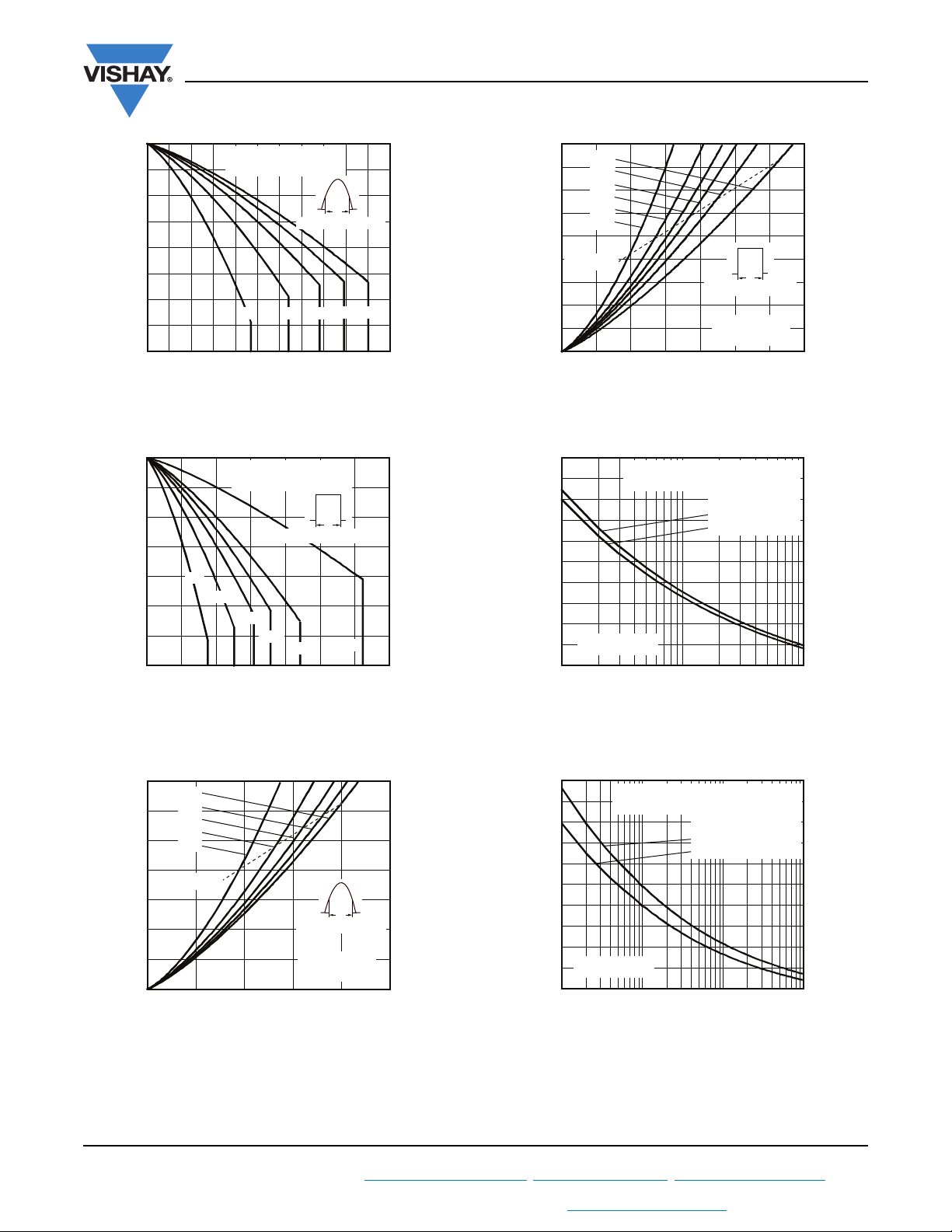
Fig. 1 - Current Rating Characteristics
Fig. 4 - Forward Power Loss Characteristics
300
250
200
150
At any rated load condition and with
rated V
applied following surge.
RRM
Initial TJ = 150 °C
at 60 Hz 0.0083 s
at 50 Hz 0.0100 s
Fig. 2 - Current Rating Characteristics
Revision: 17-Aug-11
For technical questions within your region: DiodesAmericas@vishay.com
THIS DOCUMENT IS SUBJECT TO CHANGE WITHOUT NOTICE. THE PRODUCTS DESCRIBED HEREIN AND THIS DOCUMENT
Fig. 3 - Forward Power Loss Characteristics
Forward Current (A)
Peak Half Sine Wave
100
20ETF.. Series
50
1 10 100
Number of Equal Amplitude Half Cycle
Current Pulses (N)
Fig. 5 - Maximum Non-Repetitive Surge Current
ARE SUBJECT TO SPECIFIC DISCLAIMERS, SET FORTH AT www.vishay.com/doc?91000
3
Fig. 6 - Maximum Non-Repetitive Surge Current
, DiodesAsia@vishay.com, DiodesEurope@vishay.com
Document Number: 94097
 Loading...