

20777
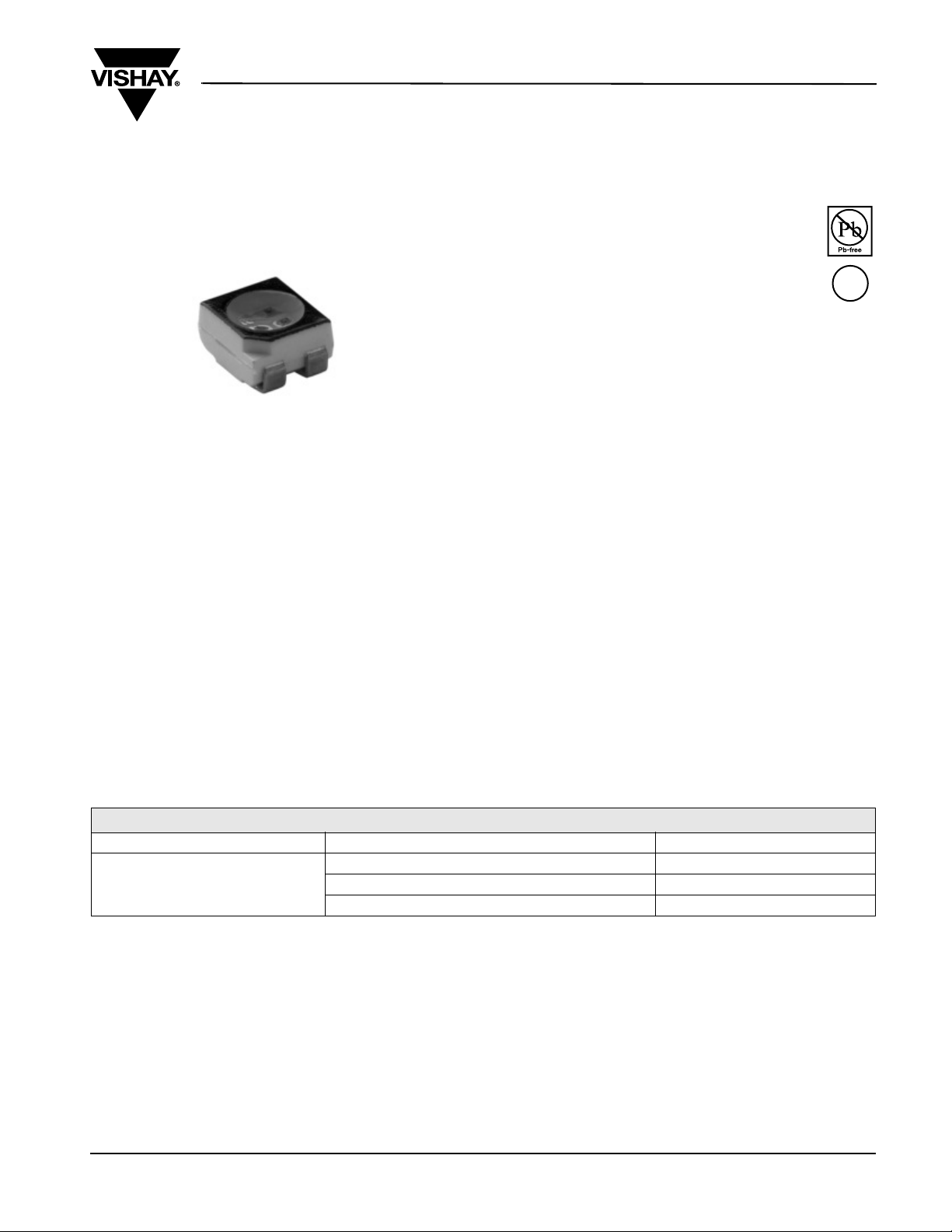
Multi SMD LED RGB
FEATURES
• High brightness tricolor SMD LED
• RGB individual control
• Compact package outline
• Black surface
• Qualified according to JEDEC moisture
sensitivity level 2
• Compatible to IR reflow soldering
• Automotive qualified AEC-Q101
• Component in accordance to RoHS 2002/95/EC
and WEEE 2002/96/EC
•
ESD-withstand voltage: up to 1 kV according to
JESD22-A114-B
VLMRGB343..
Vishay Semiconductors
e3
DESCRIPTION
VLMRGB343.. tricolor LEDs is a high brightness
device designed for demanding applications in
efficiency and reduced space. An ideal device in
emphasizing visual effects, advertisement, decoration
as well as general backlighting needs.
PRODUCT GROUP AND PACKAGE DATA
APPLICATIONS
• Wide range of accent and decorative lighting
• Displays: full color message and displays video
boards
• Consumer appliances: backlight LCDs, PDAs, TVs
• Industry: white goods such as ovens, microwaves,
etc.
• Product group: LED
• Package: SMD PLCC-4
• Product series: RGB
• Angle of half intensity: ± 60°
PARTS TABLE
PART
VLMRGB343-ST-UV-RS
Note:
Reel comes in a quantity of 2050 units per reel. Luminous intensity is measured with an accuracy of ± 11%. All electrical and optical data are
measured at room temperature of 25 °C.
COLOR (λd), LUMINOUS INTENSITY
Red, I
= (140 to 285) mcd, (typ 625 nm)
V
True green, I
Blue, I
= (285 to 560) mcd, (typ 525 nm)
V
= (100 to 200) mcd, (typ 470 nm)
V
TECHN OLO GY
AlInGaP
InGaN
InGaN
Document Number 81742
Rev. 1.3, 07-Mar-08
www.vishay.com
1
VLMRGB343..
Vishay Semiconductors
ABSOLUTE MAXIMUM RATINGS 1) VLMRGB343.., RED
PARAMETER TEST CONDITION SYMBOL VAL UE UNIT
Forward current
Reverse voltage
Power dissipation
Junction temperature
Surge current
t
< 10 µs, duty cycle = 0.005
p
Thermal resistance junction/solder point
1 chip ON
3 chip ON
Thermal resistance junction/ambient
1 chip ON
3 chip ON
Operating temperature
Storage temperature
Forward voltage 20 mA
Note:
1)
T
= 25 °C, unless otherwise specified
amb
I
F
V
R
P
tot
T
j
I
FM
R
thJP
30 mA
12 V
75 mW
125 °C
1000 mA
260
420
R
thJA
480
770
T
amb
T
stg
V
F
- 40 to + 100 °C
- 40 to + 100 °C
1.8 to 2.45 V
K/W
K/W
ABSOLUTE MAXIMUM RATINGS 1) VLMRGB343.., TRUE GREEN, BLUE
PARAMETER TEST CONDITION SYMBOL VAL UE UNIT
Forward current
Reverse voltage
Power dissipation
Junction temperature
Surge current
t
< 10 µs, duty cycle = 0.005
p
Thermal resistance junction/solder point
1 chip ON
3 chip ON
Thermal resistance junction/ambient
1 chip ON
3 chip ON
Operating temperature
Storage temperature
Forward voltage 20 mA
Note:
1)
T
= 25 °C, unless otherwise specified
amb
I
F
V
R
P
tot
T
j
I
FM
R
thJP
R
thJA
T
amb
T
stg
V
F
20 mA
5V
85 mW
125 °C
200 mA
290
470
530
820
- 40 to + 100 °C
- 40 to + 100 °C
3.7 to 4.25 V
K/W
K/W
www.vishay.com
2
Document Number 81742
Rev. 1.3, 07-Mar-08
VLMRGB343..
Vishay Semiconductors
OPTICAL AND ELECTRICAL CHARACTERISTICS 1) VLMRGB343.., RED, TRUE GREEN, BLUE
PARAMETER
TEST
CONDITION
Luminous
intensity
I
= 20 mA
F
Dominant
wavelength
Angle of half
intensity
Forward
voltage
Note:
Not designed for reverse direction
1)
T
= 25 °C, unless otherwise specified
amb
PART
VLMRGB343-
ST-UV-RS
VLMRGB343
VLMRGB343..
FLOATING
GROUPS
S3U3R3
S3U3S3
S3V3R3
S3V3S3
T3U3R3
T3U3S3
T3V3R3
T3V3S3
COLOR SYMBOL MIN. TYP. MAX. UNIT
red
I
V
140 285
mcdtrue green 285 560
blue 100 200
red
I
V
140 200
mcdtrue green 285 400
blue 100 140
red
I
V
140 200
mcdtrue green 285 400
blue 140 200
red
I
V
140 200
mcdtrue green 400 560
blue 100 140
red
I
V
140 200
mcdtrue green 400 560
blue 140 200
red
I
V
200 285
mcdtrue green 285 400
blue 100 140
red
I
V
200 285
mcdtrue green 285 400
blue 140 200
red
I
V
200 285
mcdtrue green 400 560
blue 100 140
red
I
V
200 285
mcdtrue green 400 560
blue 140 200
red
λ
d
618 625 628
blue 465 470 475
red
ϕ ± 60 degtrue green
blue
red
V
F
1.8 2.45
blue 3.6 4.25
nmtrue green 521 526 536
Vtrue green 3.7 4.25
Document Number 81742
Rev. 1.3, 07-Mar-08
www.vishay.com
3

VLMRGB343..
Vishay Semiconductors
LUMINOUS INTENSITY CLASSIFICATION RED, TRUE GREEN, BLUE
GROUP
STANDARD MIN. MAX.
R3 100 140
S3 140 200
T3 200 285
U3 285 400
V3 400 560
Note:
The standard shipping format for serial types includes a family group of 5, 6 or 9 individual brightness groups.
Individual brightness groups cannot be ordered.
COLOR CLASSIFICATION
GROUP
MIN. MAX. MIN. MAX. MIN. MAX.
618 628 521 536 465 475
A 521 526 465 470
B 526 531 470 475
C 531 536
Note:
Wavelengths are tested at a current pulse duration of 25 ms and an accuracy of ± 1 nm. Only one wavelength group is allowed for each chip
within one reel.
1)
No color grouping for red. Only for check of color.
RED
1)
LUMINOUS INTENSITY IV (MCD)
DOM. WAVELENGTH (NM)
TRUE GREEN BLUE
TYPICAL CHARACTERISTICS
= 25 °C, unless otherwise specified
T
amb
35
30
25
20
15
10
Forward Current (mA)
5
0
0 1020304050607080 90 100
20789
Ambient Temperature (°C)
Figure 1. Forward Current vs.
Ambient Temperature (1 Chip On)
true green
red
blue
35
30
25
20
15
red
true green
blue
10
Forward Current (mA)
5
0
0102030405060708 0 90 100
20790
Ambient Temperature (°C)
Figure 2. Forward Current vs.
Ambient Temperature (3 Chips On)
www.vishay.com
4
Document Number 81742
Rev. 1.3, 07-Mar-08

VLMRGB343..
Vishay Semiconductors
1.2
blue
1.0
0.8
0.6
0.4
- Rel. Luminous Intensity
0.2
V rel
I
0.0
400 450 500 550 600 650 700 750 800
20787
true green
red
- Wavelength (nm)
λ
Figure 3. Relative Intensity vs. Wavelength
35
30
red
25
true green
blue
20
15
1.01
1.005
λ
1
0.995
0.99
true green
0.985
Rel. Dominant Wavelength (nm)
0.98
20786
0102030405060
IF - Forward Current (mA)
Figure 6. Relative Dominant Wavelength vs.
Forward Current
35
30
25
20
15
red
true green
blue
10
Forward Current (mA)
5
0
1.522.533.54
20788
Forward Voltage (V)
Figure 4. Forward Current vs. Forward Voltage
2.5
2
1.5
1
- Rel. Lumnious Intensity
0.5
V rel
I
0
0102030405060
20785
IF - Forward Current (mA)
red
blue
true green
Figure 5. Relative Luminous Intensity vs.
Forward Current
10
Forward Current (mA)
5
0
0 1020304050607080 90 100
20791
Solder Point Temperature (°C)
blue
Figure 7. Forward Current vs.
Solder Point Temperature (1 Chip On)
35
30
red
25
20
15
true green
blue
10
Forward Current (mA)
5
0
01020304050607080 90 100
20792
Solder Point Temperature (°C)
Figure 8. Forward Current vs.
Solder Point Temperature (3 Chips On)
Document Number 81742
Rev. 1.3, 07-Mar-08
www.vishay.com
5

VLMRGB343..
Vishay Semiconductors
TAPING DIMENSIONS in millimeters
20819
PACKAGE DIMENSIONS/SOLDERING PADS DIMENSIONS in millimeters
www.vishay.com
6
20820
Document Number 81742
Rev. 1.3, 07-Mar-08

VLMRGB343..
255
240 °C
217 °C
Vishay Semiconductors
SOLDERING PROFILE
IR Reflow Soldering Profile for lead (Pb)-free soldering
300
250
200
150
Temperature (°C)
100
50
0
0 50 100 150 200 250 300
19470-4
Figure 9. Vishay Lead (Pb)-free Reflow Soldering Profile
Preconditioning acc. to JEDEC Level 2
255 °C
max. 120 s
max. Ramp Up 3 °C/s
(acc. to J-STD-020C)
max. 30 s
max. 100 s
max. Ramp Down 6 °C/s
Time (s)
max. 2 cycles allowed
BAR CODE PRODUCT LABEL
EXAMPLE:
A
max. 260 °C
245 °C
DRY PACKING
The reel is packed in an anti-humidity bag to protect
the devices from absorbing moisture during
transportation and storage.
Aluminum bag
Label
Reel
15973
FINAL PACKING
The sealed reel is packed into a cardboard box. A
secondary cardboard box is used for shipping
purposes.
E
C
B
A) Type of component
B) Manufacturing plant
C) SEL - selection code (bin):
e.g.: DA = code for luminous intensity group
5 = code for color group
4 = code for forward voltage
D) Batch:
200707 = year 2007, week 07
PH19 = plant code
E) Total quantity
D
20613
Document Number 81742
Rev. 1.3, 07-Mar-08
www.vishay.com
7

VLMRGB343..
Vishay Semiconductors
RECOMMENDED METHOD OF STORAGE
Dry box storage is recommended as soon as the
aluminum bag has been opened to prevent moisture
absorption. The following conditions should be
observed, if dry boxes are not available:
• Storage temperature 10 °C to 30 °C
• Storage humidity ≤ 60 % RH max.
After more than 72 h under these conditions moisture
content will be too high for reflow soldering.
In case of moisture absorption, the devices will recover
to the former condition by drying under the following
condition:
192 h at 40 °C + 5 °C/- 0 °C and < 5 % RH
(dry air/nitrogen) or
96 h at 60 °C + 5 °C and < 5 % RH for all device
containers or
24 h at 100 °C + 5 °C not suitable for reel or tubes.
An EIA JEDEC standard JESD22-A112 level 2 label is
included on all aluminum dry bags.
17028
Example of JESD22-A112 level 2 label
ESD PRECAUTION
Proper storage and handling procedures should be
followed to prevent ESD damage to the devices
especially when they are removed from the antistatic
shielding bag. Electro-static sensitive devices warning
labels are on the packaging.
VISHAY SEMICONDUCTORS STANDARD
BAR CODE LABELS
The Vishay Semiconductors standard bar code labels
are printed at final packing areas. The labels are on
each packing unit and contain Vishay Semiconductors
specific data.
www.vishay.com
8
Document Number 81742
Rev. 1.3, 07-Mar-08

VLMRGB343..
Vishay Semiconductors
OZONE DEPLETING SUBSTANCES POLICY STATEMENT
It is the policy of Vishay Semiconductor GmbH to
1. Meet all present and future national and international statutory requirements.
2. Regularly and continuously improve the performance of our products, processes, distribution and operating
systems with respect to their impact on the health and safety of our employees and the public, as well as their
impact on the environment.
It is particular concern to control or eliminate releases of those substances into the atmosphere which are known as
ozone depleting substances (ODSs).
The Montreal Protocol (1987) and its London Amendments (1990) intend to severely restrict the use of ODSs and
forbid their use within the next ten years. Various national and international initiatives are pressing for an earlier ban
on these substances.
Vishay Semiconductor GmbH has been able to use its policy of continuous improvements to eliminate the use of
ODSs listed in the following documents.
1. Annex A, B and list of transitional substances of the Montreal Protocol and the London Amendments respectively.
2. Class I and II ozone depleting substances in the Clean Air Act Amendments of 1990 by the Environmental
Protection Agency (EPA) in the USA.
3. Council Decision 88/540/EEC and 91/690/EEC Annex A, B and C (transitional substances) respectively.
Vishay Semiconductor GmbH can certify that our semiconductors are not manufactured with ozone depleting
substances and do not contain such substances.
The IEC/EN standards require that the desired classification Accessible Emission Limit shall not be exceeded
in “Normal” and “Single Fault Conditions”. This product is in Compliance with the requirement in
CEN/IEC/EN60825-1 to ensure that required classifications are not exceeded in single fault conditions.
We reserve the right to make changes to improve technical design
and may do so without further notice.
Parameters can vary in different applications. All operating parameters must be validated for each customer
application by the customer. Should the buyer use Vishay Semiconductors products for any unintended or
unauthorized application, the buyer shall indemnify Vishay Semiconductors against all claims, costs, damages, and
expenses, arising out of, directly or indirectly, any claim of personal damage, injury or death associated with such
unintended or unauthorized use.
Vishay Semiconductor GmbH, P.O.B. 3535, D-74025 Heilbronn, Germany
Document Number 81742
Rev. 1.3, 07-Mar-08
www.vishay.com
9

Legal Disclaimer Notice
Vishay
Notice
Specifications of the products displayed herein are subject to change without notice. Vishay Intertechnology, Inc.,
or anyone on its behalf, assumes no responsibility or liability for any errors or inaccuracies.
Information contained herein is intended to provide a product description only. No license, express or implied, by
estoppel or otherwise, to any intellectual property rights is granted by this document. Except as provided in Vishay's
terms and conditions of sale for such products, Vishay assumes no liability whatsoever, and disclaims any express
or implied warranty, relating to sale and/or use of Vishay products including liability or warranties relating to fitness
for a particular purpose, merchantability, or infringement of any patent, copyright, or other intellectual property right.
The products shown herein are not designed for use in medical, life-saving, or life-sustaining applications.
Customers using or selling these products for use in such applications do so at their own risk and agree to fully
indemnify Vishay for any damages resulting from such improper use or sale.
Document Number: 91000 www.vishay.com
Revision: 08-Apr-05 1
 Loading...