

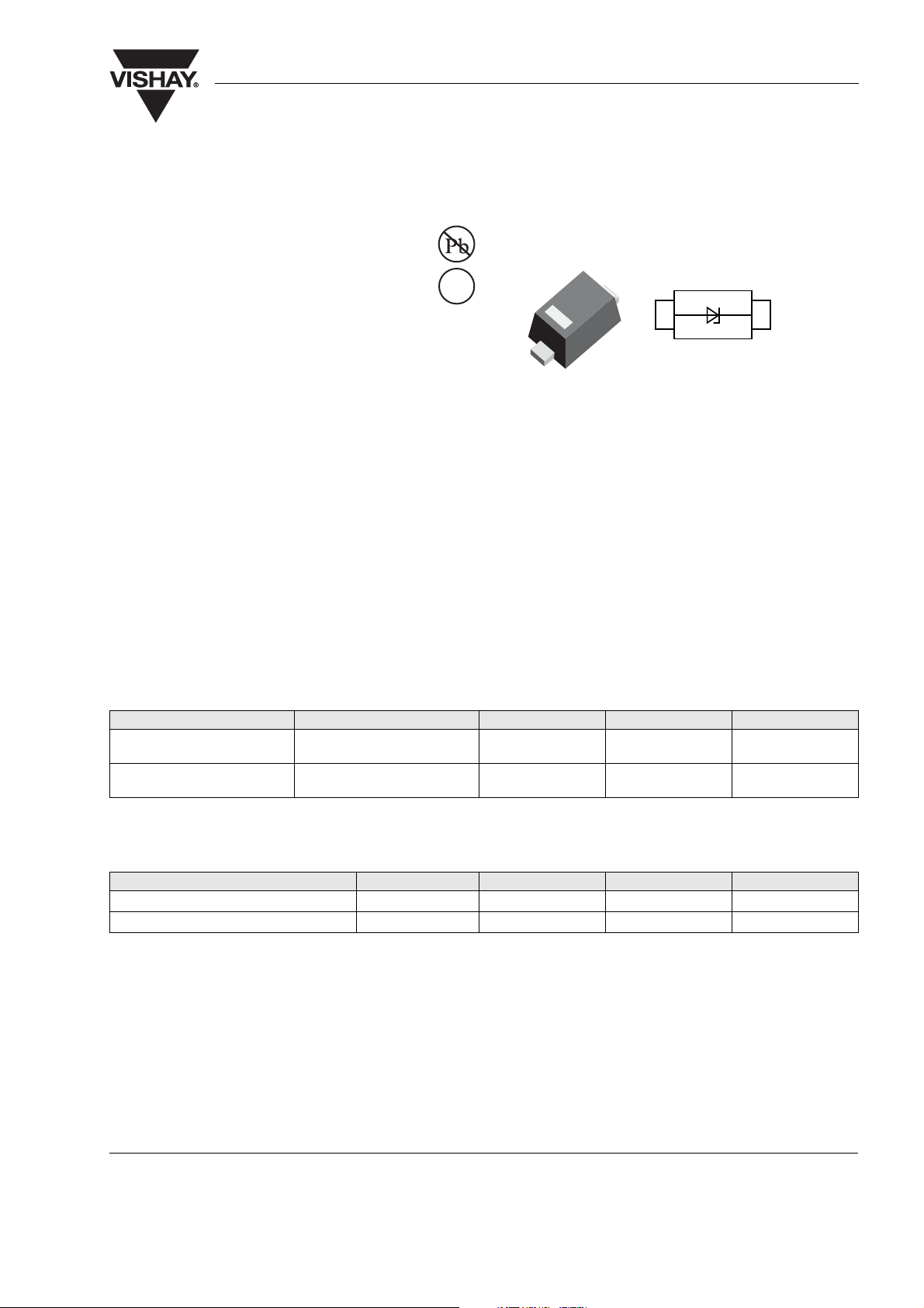
Single ESD Protection Diode in SOD-523
Features
• Small SOD-523 package
• Low leakage current
• ESD protection to IEC 61000-4-2 15 kV (air)
• ESD protection to IEC 61000-4-2 8 kV (contact)
• Lead (Pb)-free component
• Component in accordance to RoHS 2002/95/EC
and WEEE 2002/96/EC
Mechanical Data
Case: SOD-523 Plastic case
Molding Compound Flammability Rating:
UL 94 V-0
Terminals: High temperature soldering guaranteed:
260 °C/10 sec. at terminals
Weight: approx. 1.6 mg
Packaging Codes/Options:
GS18 / 10 k per 13" reel (8 mm tape), 10 k/box
GS08 / 3 k per 7" reel (8 mm tape), 15 k/box
e3
2
VESDxx-02V
Vishay Semiconductors
1
1 2
18554
Absolute Maximum Ratings
Ratings at 25 °C, ambient temperature unless otherwise specified
Parameter Test condition Symbol Val ue Unit
ESD Air discharge per
IEC 61000-4-2
ESD Contact discharge per
IEC 61000-4-2
Thermal Characteristics
Ratings at 25 °C, ambient temperature unless otherwise specified
Parameter Test condition Symbol Val ue Unit
Operating temperature T
Storage temperature T
V
ESD
V
ESD
J
STG
15 kV
8kV
- 40 to + 125 °C
- 55 to + 150 °C
Document Number 85857
Rev. 1.2, 02-May-05
www.vishay.com
1
VESDxx-02V
Vishay Semiconductors
Electrical Characteristics
Partnumber Marking Code Reverse
Stand-off
Voltage
@ I
Rmax
V
RWM
V μA V A V pF
VESD01-02V
VESD03-02V
VESD05-02V
VESD08-02V
VESD12-02V
A*
B*
C*
D*
E*
)
)
)
)
)
1 100 9 7 1.5 180
3 2012 9 4110
50.120 66.555
8 0.1 30 4 9 35
12 0.1 25 2 14 30
*) Number turned by 180°
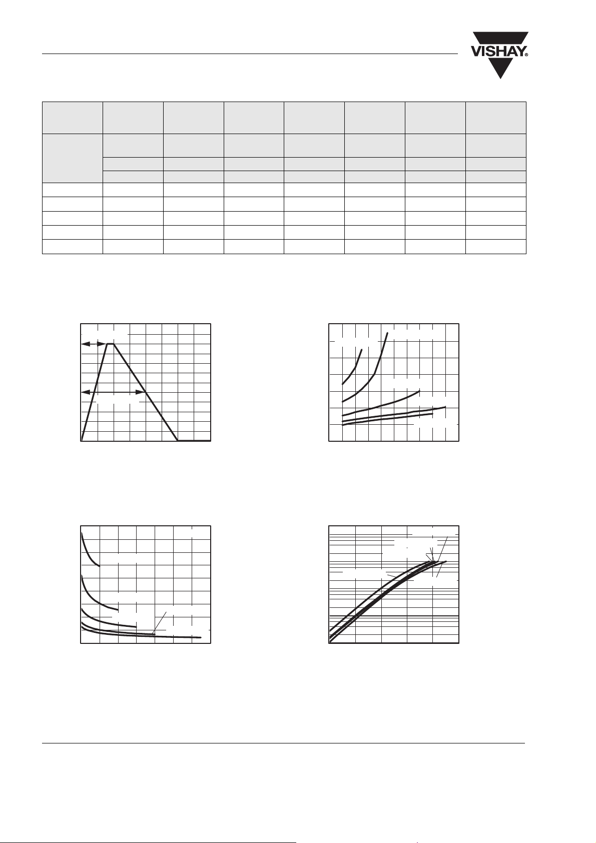
Typical Characteristics (Tamb = 25 °C unless otherwise specified)
Max.
Reverse
Current
@ V
RWM
I
R
Max.
Clamping
Voltage
@ I
PPM
(see Fig. 1)
V
C
Max. Peak
Pulse
Current
(see Fig. 1) @ IR = 1 mA @ VR = 0 V,
I
PPM
Min. Reverse
Breakdown
Voltage
V
BR
Capacitance
f = 1 MHZ
C
D
120
8 μsto100%
100
80
60
20 μsto50%
40
- Peak Pulse Current(%)
20
PP
I
0
0 5 10 15 20 25 30 35 40
19015
t - Time ( μ s)
Figure 1. Pulse Waveform 8/20 μs acc. IEC 61000 - 4 - 5
180
160
19011
140
120
100
80
60
40
D
C - Diode Capacitance ( pF )
20
0
VESD01-02V
VESD03-02V
VESD05-02V
02468101214
VR- Reverse Voltage(V)
f=1MHz
VESD08-02V
VESD12-02V
35
30
VESD12-02V
25
20
15
10
C
5
V - Clamping Voltage ( V )
0
012345678910
19014
I
PP
VESD08-02V
VESD05-02V
VESD03-02V
VESD01-02V
- Peak Pulse Current(A)
Figure 3. Clamping Voltage vs. Peak Pulse Current
1000
100
VESD01-02V
10
1
F
I - Forward Current ( mA )
0.1
0.7 0.75 0.8 0.85 0.9 0.95
19012
VF- Forward Voltage(V)
VESD03-02V
VESD12-02V
VESD08-02V
VESD05-02V
Figure 2. Typ. Diode Capacitance vs. Reverse Voltage
www.vishay.com
2
Figure 4. Forward Current vs. Forward Voltage
Document Number 85857
Rev. 1.2, 02-May-05

VESDxx-02V
Vishay Semiconductors
18
16
VESD12-02V
14
12
VESD08-02V
10
8
VESD05-02V
6
4
19013
R
V - Reverse Voltage(V)
VESD03-02V
2
0
0.01 0.1 1 10 100 1000
IR- Reverse Current ( μA)
VESD01-02V
Figure 5. Reverse Voltage vs. Reverse Current
Package Dimensions in mm (Inches)
ISO Method E
0.15 (0.006)
10
9
8
7
6
5
4
3
F
2
V - Forward Voltage ( V )
1
0
0 2 4 6 8 101214161820
19061
VESD01-02V
IPP- Peak Pulse Current(A)
VESD12-02V
VESD03-02V
VESD05-02V
VESD08-02V
Figure 6. Typical Forward Voltage vs. Peak Pulse Current
0.6 (0.023)
0.3 (0.012)
0.22 (0.008)
0.16 (0.006)
1.6 (0.062)
1.2 (0.047)
A
0.8 (0.031)
Mounting Pad Layout
1.35 (0.053)
0.15 A
0.39 (0.015)
0.35 (0.014)
16864
Document Number 85857
Rev. 1.2, 02-May-05
www.vishay.com
3

VESDxx-02V
Vishay Semiconductors
Ozone Depleting Substances Policy Statement
It is the policy of Vishay Semiconductor GmbH to
1. Meet all present and future national and international statutory requirements.
2. Regularly and continuously improve the performance of our products, processes, distribution and operating
systems with respect to their impact on the health and safety of our employees and the public, as well as
their impact on the environment.
It is particular concern to control or eliminate releases of those substances into the atmosphere which are
known as ozone depleting substances (ODSs).
The Montreal Protocol (1987) and its London Amendments (1990) intend to severely restrict the use of ODSs
and forbid their use within the next ten years. Various national and international initiatives are pressing for an
earlier ban on these substances.
Vishay Semiconductor GmbH has been able to use its policy of continuous improvements to eliminate the use
of ODSs listed in the following documents.
1. Annex A, B and list of transitional substances of the Montreal Protocol and the London Amendments
respectively
2. Class I and II ozone depleting substances in the Clean Air Act Amendments of 1990 by the Environmental
Protection Agency (EPA) in the USA
3. Council Decision 88/540/EEC and 91/690/EEC Annex A, B and C (transitional substances) respectively.
Vishay Semiconductor GmbH can certify that our semiconductors are not manufactured with ozone depleting
substances and do not contain such substances.
We reserve the right to make changes to improve technical design
and may do so without further notice.
Parameters can vary in different applications. All operating parameters must be validated for each
customer application by the customer. Should the buyer use Vishay Semiconductors products for any
unintended or unauthorized application, the buyer shall indemnify Vishay Semiconductors against all
claims, costs, damages, and expenses, arising out of, directly or indirectly, any claim of personal
damage, injury or death associated with such unintended or unauthorized use.
Vishay Semiconductor GmbH, P.O.B. 3535, D-74025 Heilbronn, Germany
www.vishay.com
4
Document Number 85857
Rev. 1.2, 02-May-05

Legal Disclaimer Notice
Vishay
Notice
Specifications of the products displayed herein are subject to change without notice. Vishay Intertechnology, Inc.,
or anyone on its behalf, assumes no responsibility or liability for any errors or inaccuracies.
Information contained herein is intended to provide a product description only. No license, express or implied, by
estoppel or otherwise, to any intellectual property rights is granted by this document. Except as provided in Vishay's
terms and conditions of sale for such products, Vishay assumes no liability whatsoever, and disclaims any express
or implied warranty, relating to sale and/or use of Vishay products including liability or warranties relating to fitness
for a particular purpose, merchantability, or infringement of any patent, copyright, or other intellectual property right.
The products shown herein are not designed for use in medical, life-saving, or life-sustaining applications.
Customers using or selling these products for use in such applications do so at their own risk and agree to fully
indemnify Vishay for any damages resulting from such improper use or sale.
Document Number: 91000 www.vishay.com
Revision: 08-Apr-05 1
 Loading...