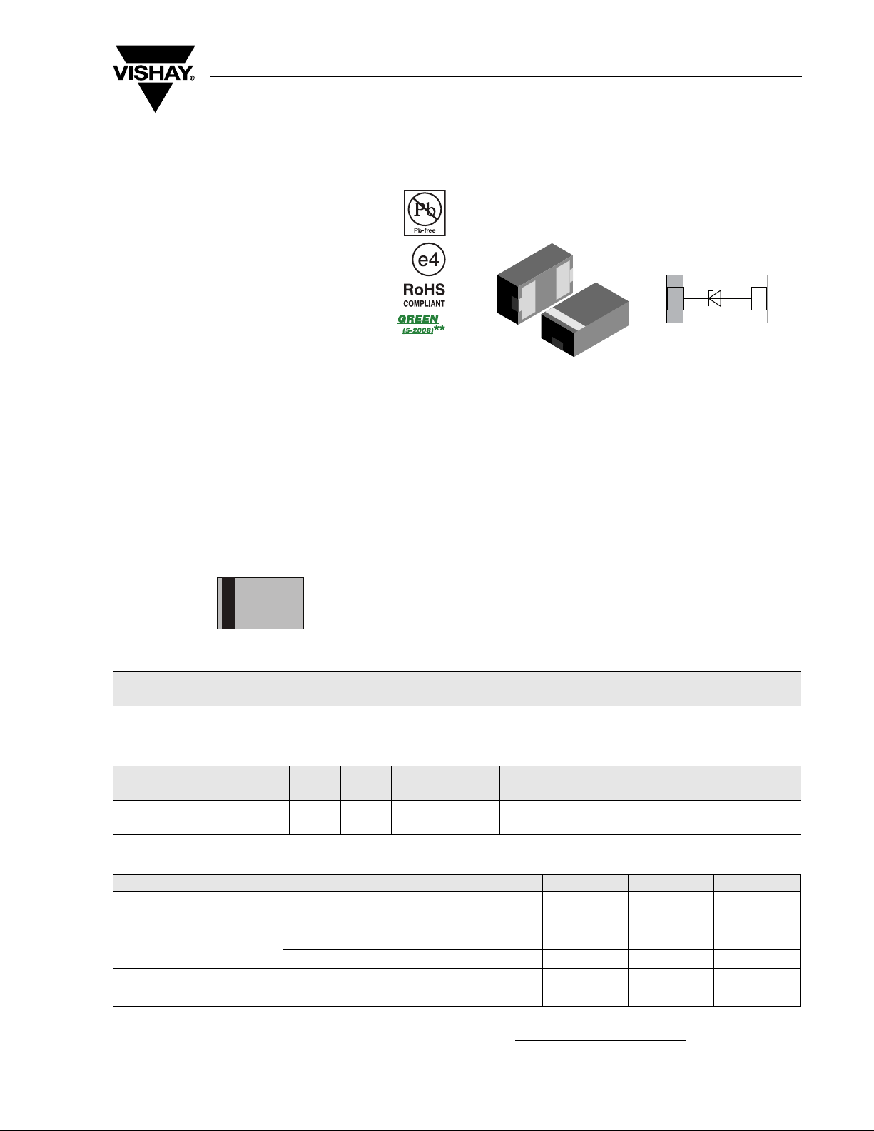
ESD-Protection Diode in LLP1006-2L
Features
• Ultra compact LLP1006-2L package
• Low package height < 0.4 mm
• 1-line ESD-protection
• Low leakage current < 0.1 µA
• Low load capacitance C
(V
= 2.5 V; f = 1 MHz)
R
• ESD-protection acc. IEC 61000-4-2
± 30 kV contact discharge
± 30 kV air discharge
• High surge current acc. IEC61000-4-5 I
• Soldering can be checked by standard vision
inspection. No X-ray necessary
• AEC Q101 qualified
• Lead (Pb)-free component
• Pin plating NiPdAu (e4) no whisker growth
• Component in accordance to RoHS 2002/95/EC
and WEEE 2002/96/EC
= 12 pF
D
PP
> 3 A
VESD05A1B-HD1
Vishay Semiconductors
2
20855
1
20856
Marking (example only)
Bar = Cathode marking
XY
21121
X = Date code
Y = Type code (see table below)
Ordering Information
Device name Ordering code
VESD05A1B-HD1 VESD05A1B-HD1-GS08 8000 8000
Taped units per reel
(8 mm tape on 7" reel)
Minimum order quantity
Package Data
Device name
VESD05A1B-HD1 LLP1006-2L D 0.72 mg UL 94 V-0
Package
name
Type
code
Weight
Molding compound
flammability rating
Moisture sensitivity level Soldering conditions
MSL level 1
(according J-STD-020)
260 °C/10 s at terminals
Absolute Maximum Ratings
Rating Test conditions Symbol Val ue Unit
Peak pulse current
Peak pulse power
ESD immunity
Operating temperature Junction temperature
Storage temperature
Acc. IEC 61000-4-5, t
Acc. IEC 61000-4-5, t
Contact discharge acc. IEC 61000-4-2; 10 pulses
Air discharge acc. IEC 61000-4-2; 10 pulses
= 8/20 µs/single shot I
P
= 8/20 µs/single shot P
P
V
V
T
PPM
PP
ESD
ESD
T
STG
3A
33 W
± 30 kV
± 30 kV
J
- 40 to + 125 °C
- 55 to + 150 °C
** Please see document “Vishay Green and Halogen-Free Definitions (5-2008)” http://www.vishay.com/doc?99902
Document Number 81796
Rev. 1.3, 27-Oct-08
For technical support, please contact: ESD-Protection@vishay.com
www.vishay.com
1

VESD05A1B-HD1
Vishay Semiconductors
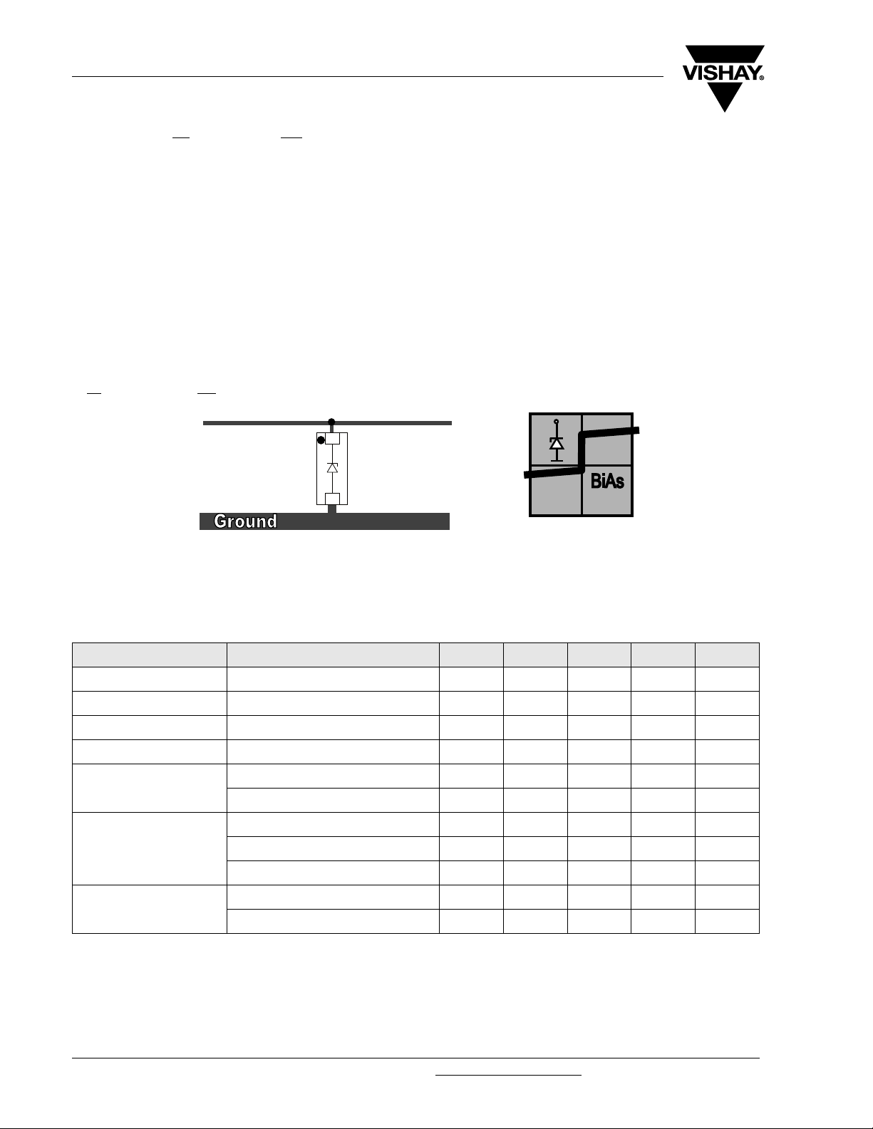
BiAs-Mode (Bidirectional Asymmetrical protection mode)
With the VESD05A1B-HD1 one signal- or data-lines (L1) can be protected against voltage transients. With
pin 1 connected to ground and pin 2 connected to a signal- or data-line which has to be protected. As long as
the voltage level on the data- or signal-line is between 0 V (ground level) and the specified Maximum Reverse
Working Voltage (V
line. The protection device behaves like an open switch.
As soon as any positive transient voltage signal exceeds the break through voltage level of the protection
diode, the diode becomes conductive and shorts the transient current to ground. Now the protection device
behaves like a closed switch. The Clamping Voltage (V
plus the voltage drop at the series impedance (resistance and inductance) of the protection device.
Any negative transient signal will be clamped accordingly. The negative transient current is flowing in the
forward direction of the protection diode. The low Forward Voltage (V
the ground level.
Due to the different clamping levels in forward and reverse direction the VESD05A1B-HD1 clamping behaviour
is Bi
directional and Asymmetrical (BiAs).
) the protection diode between data line and ground offers a high isolation to the ground
RWM
) is defined by the BReakthrough Voltage (VBR) level
C
) clamps the negative transient close to
F
L1
2
1
Electrical Characteristics
Ratings at 25 °C ambient temperature, unless otherwise specified
VESD05A1B-HD1
BiAs mode (between pin 1 and pin 2)
Parameter Test conditions/remarks Symbol Min. Ty p. Max. Unit
Protection paths Number of lines which can be protected
at I
Reverse stand off voltage
Reverse current
Reverse break down voltage
Reverse clamping voltage
Forward clamping voltage
Capacitance
at V
at V
= 0.1 µA V
R
= 5 V I
at V
R
at I
= 1 mA V
R
= 1 A V
at I
PP
at I
= I
PP
at I
at I
at I
PP
= 0 V; f = 1 MHz C
R
= 2.5 V; f = 1 MHz C
R
= 3 A V
PPM
= 0.2 A V
PP
= 1 A V
PP
= I
= 3 A V
PPM
N
lines
RWM
R
BR
C
C
F
F
F
D
D
20925
1 lines
5V
0.01 0.1 µA
66.87.5V
89.5V
8.9 11 V
0.95 1.2 V
1.3 V
1.9 V
19 23 pF
12 pF
www.vishay.com
2
For technical support, please contact: ESD-Protection@vishay.com
Document Number 81796
Rev. 1.3, 27-Oct-08

Typical Characteristics
T
= 25 °C, unless otherwise specified
amb
VESD05A1B-HD1
Vishay Semiconductors
120 %
100 %
ESD
Discharge Current I
20557
80 %
60 %
53 %
40 %
27 %
20 %
0 %
- 10 0 10 20 30 40 50 60 70 80 90 100
Rise time = 0.7 ns to 1 ns
Time (ns)
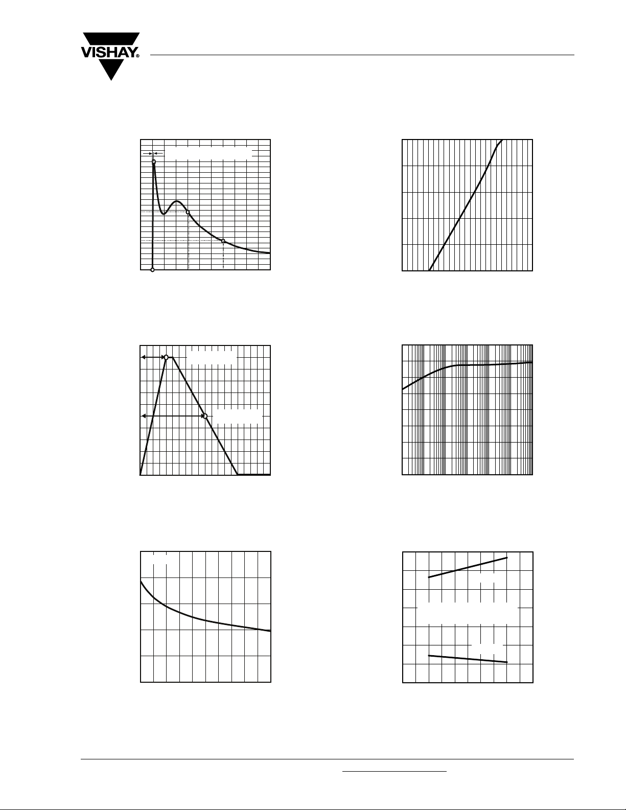
Figure 1. ESD Discharge Current Wave Form
acc. IEC 61000-4-2 (330 Ω/150 pF)
8 µs to 100 %
20 µs to 50 %
Time (µs)
I
100 %
80 %
60 %
PPM
40 %
20 %
0 %
010203040
20548
Figure 2. 8/20 µs Peak Pulse Current Wave Form
acc. IEC 61000-4-5
100
10
1
(mA)
F
I
0.1
0.01
0.001
21157
0.5 10.80.70.6
VF (V)
0.9
Figure 4. Typical Forward Current IF vs. Forward Voltage V
8
7
6
5
(V)
4
R
V
3
2
1
21158
0
0.01 1001010.1
IR (µA)
1000
10000
Figure 5. Typical Reverse Voltage VR vs. Reverse Current I
F
R
25
f = 1 MHz
20
15
(pF)
D
C
10
5
0
04321
21156
Figure 3. Typical Capacitance C
Document Number 81796
Rev. 1.3, 27-Oct-08
10
8
6
4
Measured acc. IEC 61000-4-5
(8/20 µs - wave form)
2
0
- 2
- 4
012345
VR (V)
vs. Reverse Voltage V
D
(V)
C
/V
F
V
5
21159
R
Figure 6. Typical Clamping Voltage vs. Peak Pulse Current I
For technical support, please contact: ESD-Protection@vishay.com
reverse
forward
IPP (A)
PP
www.vishay.com
3
 Loading...