

www.vishay.com
16758-10
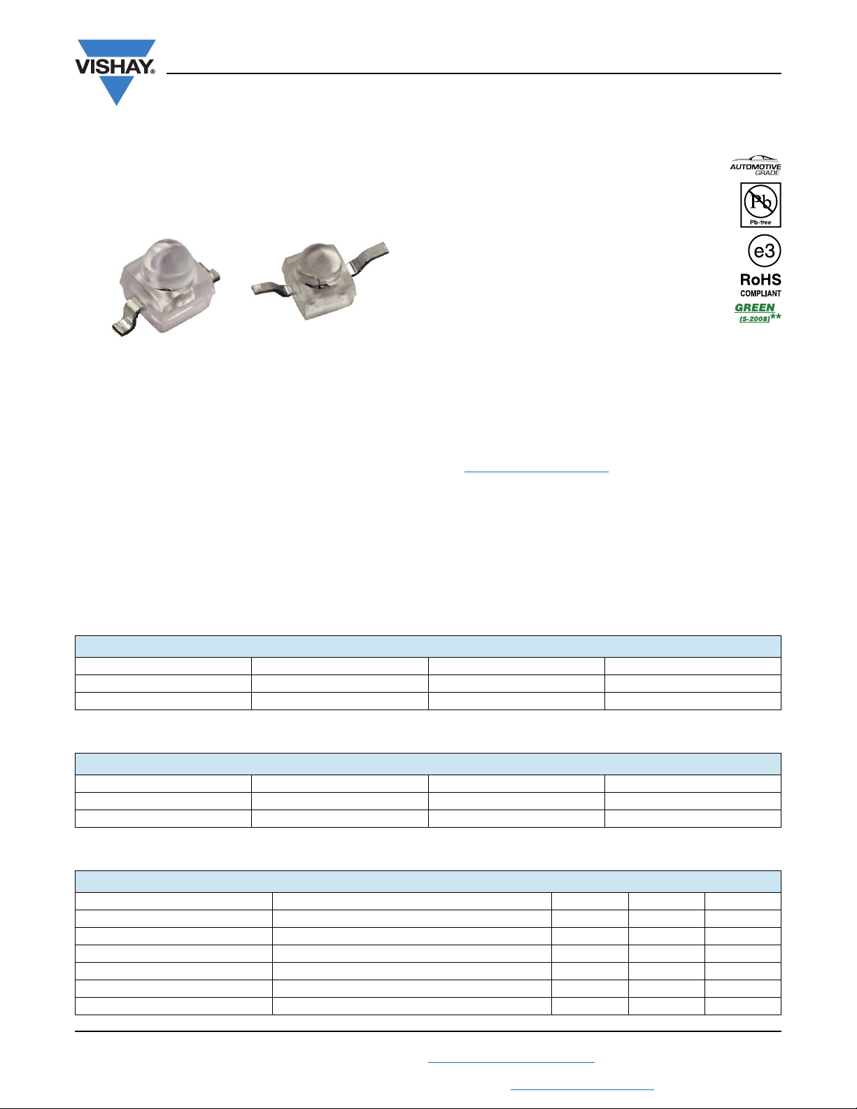
VEMT2500X01VEMT2520X01
Silicon NPN Phototransistor
DESCRIPTION
VEMT2500X01 series are silicon NPN epitaxial planar
phototransistors in a miniature dome lens, clear epoxy
package for surface mounting. The device is sensitive to
visible and near infrared radiation.
VEMT2500X01, VEMT2520X01
Vishay Semiconductors
FEATURES
• Package type: surface mount
• Package form: GW, RGW
• Dimensions (L x W x H in mm): 2.3 x 2.3 x 2.8
• AEC-Q101 qualified
• High radiant sensitivity
• Suitable for visible and near infrared radiation
• Fast response times
• Angle of half sensitivity: = ± 15°
• Package matched with IR emitter series
VSMB2000X01
• Floor life: 4 weeks, MSL 2a, acc. J-STD-020
• Lead (Pb)-free reflow soldering
• Compliant to RoHS Directive 2002/95/EC and in
accordance to WEEE 2002/96/EC
Note
** Please see document “Vishay Material Category Policy”:
www.vishay.com/doc?99902
APPLICATIONS
• Detector in automotive applications
• Photo interrupters
• Miniature switches
•Counters
•Encoders
• Position sensors
PRODUCT SUMMARY
COMPONENT Ica (mA) (deg)
VEMT2500X01 6 ± 15 470 to 1090
VEMT2520X01 6 ± 15 470 to 1090
Note
• Test condition see table “Basic Characteristics”
0.1
(nm)
ORDERING INFORMATION
ORDERING CODE PACKAGING REMARKS PACKAGE FORM
VEMT2500X01 Tape and reel MOQ: 6000 pcs, 6000 pcs/reel Reverse gullwing
VEMT2520X01 Tape and reel MOQ: 6000 pcs, 6000 pcs/reel Gullwing
Note
• MOQ: minimum order quantity
ABSOLUTE MAXIMUM RATINGS (T
PARAMETER TEST CONDITION SYMBOL VALUE UNIT
Collector emitter voltage V
Emitter collector voltage V
Collector current I
Power power dissipation T
Junction temperature T
Operating temperature range T
Rev. 1.2, 24-Aug-11
THIS DOCUMENT IS SUBJECT TO CHANGE WITHOUT NOTICE. THE PRODUCTS DESCRIBED HEREIN AND THIS DOCUMENT
For technical questions, contact: detectortechsupport@vishay.com
ARE SUBJECT TO SPECIFIC DISCLAIMERS, SET FORTH AT www.vishay.com/doc?91000
= 25 °C, unless otherwise specified)
amb
75 °C P
amb
1
CEO
ECO
C
amb
20 V
7V
50 mA
V
j
100 mW
100 °C
- 40 to + 100 °C
Document Number: 81134
www.vishay.com
VEMT2500X01, VEMT2520X01
Vishay Semiconductors
ABSOLUTE MAXIMUM RATINGS (T
= 25 °C, unless otherwise specified)
amb
PARAMETER TEST CONDITION SYMBOL VALUE UNIT
Storage temperature range T
Soldering temperature Acc. reflow profile fig. 8 T
Thermal resistance junction/ambient Acc. J-STD-051 R
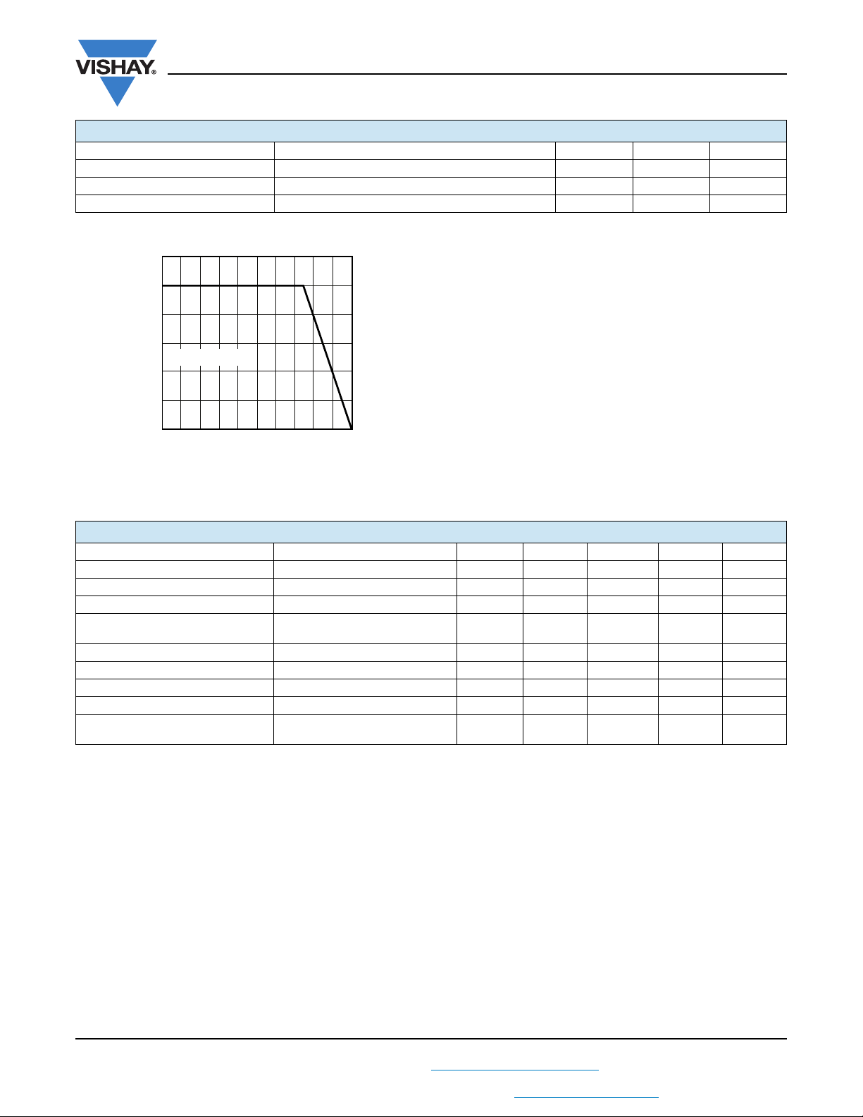
120
100
80
60
R
= 250 K/W
thJA
40
- Power Dissipation (mW)
V
20
P
0
0 10203040 50607080 90100
21619
- Ambient Temperature (°C)
T
amb
stg
sd
thJA
- 40 to + 100 °C
260 °C
250 K/W
Fig. 1 - Power Dissipation Limit vs. Ambient Temperature
BASIC CHARACTERISTICS (T
= 25 °C, unless otherwise specified)
amb
PARAMETER TEST CONDITION SYMBOL MIN. TYP. MAX. UNIT
Collector emitter breakdown voltage I
Collector dark current V
Collector emitter capacitance V
E
Collector light current
e
= 0.1 mA V
C
= 5 V, E = 0 I
CE
= 0 V, f = 1 MHz, E = 0 C
CE
= 1 mW/cm2, = 950 nm,
V
= 5 V
CE
CEO
CEO
CEO
I
CA
20 V
1 100 nA
25 pF
369mA
Angle of half sensitivity ± 15 deg
Wavelength of peak sensitivity
Range of spectral bandwidth
Collector emitter saturation voltage I
Temperature coefficient of I
ca
Ee = 1 mW/cm2, = 950 nm,
= 0.05 mA V
C
V
= 5 V
CE
Tk
p
0.1
CEsat
Ica
850 nm
470 to 1090 nm
0.4 V
1.1 %/K
Rev. 1.2, 24-Aug-11
2
Document Number: 81134
For technical questions, contact: detectortechsupport@vishay.com
THIS DOCUMENT IS SUBJECT TO CHANGE WITHOUT NOTICE. THE PRODUCTS DESCRIBED HEREIN AND THIS DOCUMENT
ARE SUBJECT TO SPECIFIC DISCLAIMERS, SET FORTH AT www.vishay.com/doc?91000
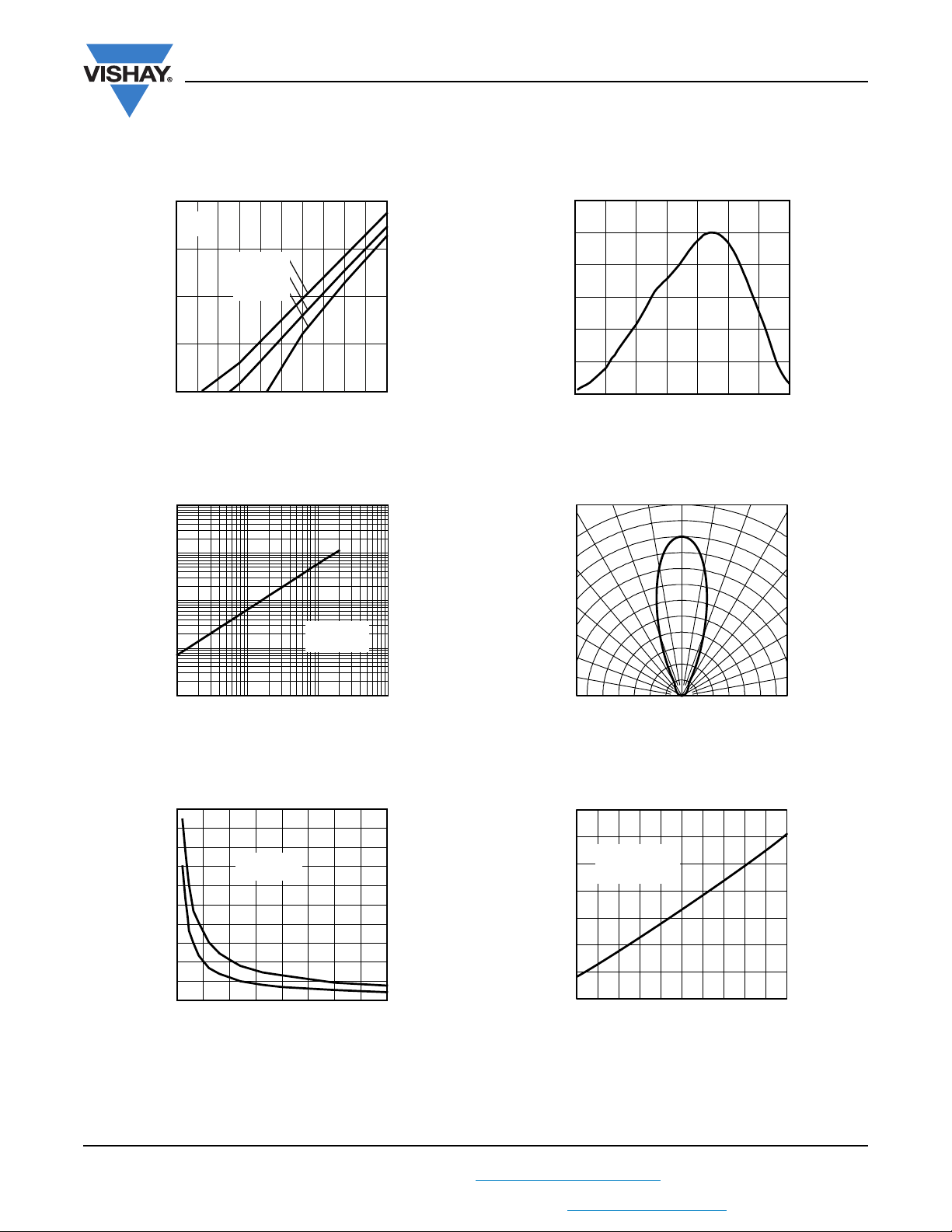
www.vishay.com
1
10
100
1000
10 000
0 102030405060708090100
T
amb
- Ambient Temperature (°C)
I
CE0
- Collector Dark Current (nA)
IF = 0
VCE = 70 V
V
CE
= 25 V
V
CE
= 5 V
20594
0
0.2
0.4
0.6
0.8
1.0
1.2
400 500 600 700 800 900 1000 1100
21555
λ - Wavelength (nm)
S (λ)
rel
- Relative Spectral Sensitivity
0
0.6
0.8
1.0
1.2
1.4
2.0
20 40 60 80
100
1.6
1.8
λ
94 8239
T
amb
- Ambient Temperature (°C)
I
ca rel
- Relative Collector Current
VCE = 5 V
E
e
= 1 mW/cm
2
= 950 nm
VEMT2500X01, VEMT2520X01
Vishay Semiconductors
BASIC CHARACTERISTICS (T
= 25 °C, unless otherwise specified)
amb
Fig. 2 - Collector Dark Current vs. Ambient Temperature
100
10
1
VCE = 5 V,
0.1
- Collector Light Current (mA)
ca
I
0.01
0.01 0.1 1 10
21573
Ee - Irradiance (mW/cm²)
λ = 950 nm
Fig. 5 - Relative Spectral Sensitivity vs. Wavelength
0°
10° 20°
1.0
0.9
0.8
- Relative Sensitivity
rel
S
0.7
94 8248
0.6
0.20.4
0
30°
40°
50°
60°
70°
ϕ - Angular Displacement
80°
Fig. 3 - Collector Light Current vs. Irradiance
100
90
80
70
60
50
40
30
- Rise/Fall Time (µs)
f
/t
r
t
20
10
Rev. 1.2, 24-Aug-11
THIS DOCUMENT IS SUBJECT TO CHANGE WITHOUT NOTICE. THE PRODUCTS DESCRIBED HEREIN AND THIS DOCUMENT
0
0 250 500 750 1000 1250 1500 1750 2000
20599
Fig. 4 - Rise/Fall Time vs. Collector Current
Fig. 6 - Relative Radiant Sensitivity vs. Angular Displacement
RL = 100 Ω
t
f
t
r
I
- Collector Current (µA)
C
Fig. 7 - Relative Collector Current vs. Ambient Temperature
3
For technical questions, contact: detectortechsupport@vishay.com
ARE SUBJECT TO SPECIFIC DISCLAIMERS, SET FORTH AT www.vishay.com/doc?91000
Document Number: 81134

www.vishay.com
0
50
100
150
200
250
300
0 50 100 150 200 250 300
Time (s)
Temperature (°C)
240 °C
245 °C
max. 260 °C
max. 120 s
max. 100 s
217 °C
max. 30 s
max. ramp up 3 °C/s
max. ramp down 6 °C/s
19841
255 °C
VEMT2500X01, VEMT2520X01
Vishay Semiconductors
REFLOW SOLDER PROFILE
Fig. 8 - Lead (Pb)-free Reflow Solder Profile acc. J-STD-020
PACKAGE DIMENSIONS VEMT2500X01 in millimeters
0.4
± 0.1
0.05
± 0.2
2.77
1.6
0
.
1
9
DRYPACK
Devices are packed in moisture barrier bags (MBB) to
prevent the products from moisture absorption during
transportation and storage. Each bag contains a desiccant.
FLOOR LIFE
Floor life (time between soldering and removing from MBB)
must not exceed the time indicated on MBB label:
Floor life: 4 weeks
Conditions: T
< 30 °C, RH < 60 %
amb
Moisture sensitivity level 2a, acc. to J-STD-020.
DRYING
In case of moisture absorption devices should be baked
before soldering. Conditions see J-STD-020 or label.
Devices taped on reel dry using recommended conditions
192 h at 40 °C (+ 5 °C), RH < 5 %.
± 0.1
Ø 1.8
0.3
Rev. 1.2, 24-Aug-11
THIS DOCUMENT IS SUBJECT TO CHANGE WITHOUT NOTICE. THE PRODUCTS DESCRIBED HEREIN AND THIS DOCUMENT
0.5
± 0.2
2.3
0.75
Drawing-No.: 6.544-5391.01-4
Issue: 1; 26.09.08
21570
Collector
2.2
± 0.2
5.8
± 0.2
2.3
1.7
6.7
Solder pad proposal
acc. IPC 7351
Ø 2.3
Exposed copper
0.4
EmitterPIN ID
± 0.1
2.2
Z 20:1
Technical drawings
according to DIN
specifications
Not indicated to lerances ±0.1
4
For technical questions, contact: detectortechsupport@vishay.com
ARE SUBJECT TO SPECIFIC DISCLAIMERS, SET FORTH AT www.vishay.com/doc?91000
± 0.1
1.1
0.254
Document Number: 81134

www.vishay.com
PACKAGE DIMENSIONS VEMT2520X01 in millimeters
VEMT2500X01, VEMT2520X01
Vishay Semiconductors
2.77 ± 0.2
1.6
0.05
0.5
2.3 ± 0.2
Collector
Solder pad proposal
acc. IPC 7351
0.75
0.4
2.2
4.2 ± 0.2
2.3 ± 0.2
Pin ID
Emitter
0.4
9
1
.
0
Exposed copper
Ø 1.8
2.2
0.3
0.6
Technical drawings
according to DIN
specifications
0.254
Not indicated tolerances ± 0.1
Document Number: 81134
Rev. 1.2, 24-Aug-11
2.45
5.15
Drawing-No.: 6.544-5383.01-4
Issue: 4; 28.01.09
21569
5
For technical questions, contact: detectortechsupport@vishay.com
THIS DOCUMENT IS SUBJECT TO CHANGE WITHOUT NOTICE. THE PRODUCTS DESCRIBED HEREIN AND THIS DOCUMENT
ARE SUBJECT TO SPECIFIC DISCLAIMERS, SET FORTH AT www.vishay.com/doc?91000

Issue: 2; 18.03.10
Drawing-No.: 9.800-5100.01-4
Leader and trailer tape:
Parts mounted
Empty (400 mm min.)
Empty (160 mm min.)
Direction of pulling out
Unreel direction
Ø 62 ± 0.5
Ø 330 ± 1
Reel
2
.
5
± 0.5
Label posted here
coming out from reel
Tape position
X
Ø
1
3
± 0.5
12.4 ± 1.5
X 2:1
I
II
6000 pcs/reel
12 ± 0.3
5.5 ± 0.05
1.75
± 0.1
2 ± 0.05
4 ± 0.1
4 ± 0.1
Ø 1.55 ± 0.05
3.05 ± 0.1
21572
Technical drawings
according to DIN
specifications
Terminal position in tape
Devicce
VEMD2000
VEMD2500
Cathode Anode
Anode Cathode
VSMB2000
VSMG2000
VSMY2850RG
VEMT2000
VEMT2500
Collector Emitter
Lead I Lead II
VEMT2500X01, VEMT2520X01
www.vishay.com
TAPE AND REEL DIMENSIONS VEMT2500X01 in millimeters
Vishay Semiconductors
Rev. 1.2, 24-Aug-11
THIS DOCUMENT IS SUBJECT TO CHANGE WITHOUT NOTICE. THE PRODUCTS DESCRIBED HEREIN AND THIS DOCUMENT
For technical questions, contact: detectortechsupport@vishay.com
ARE SUBJECT TO SPECIFIC DISCLAIMERS, SET FORTH AT www.vishay.com/doc?91000
6
Document Number: 81134

Drawing-No.: 9.800-5091.01-4
Leader and trailer tape:
Parts mounted
Empty (400 mm min.)
Empty (160 mm min.)
Direction of pulling out
Unreel direction
Ø 62 ± 0.5
Ø 330 ± 1
Reel
2
.
5
± 0.5
Label posted here
coming out from reel
Tape position
X
Ø
13
± 0.5
12.4 ± 1.5
X 2:1
I
II
6000 pcs/reel
12 ± 0.3
5.5 ± 0.05
1.75
± 0.1
2 ± 0.05
4 ± 0.1
4 ± 0.1
Ø 1.55 ± 0.05
3.05 ± 0.1
21571
technical drawings
according to DIN
specifications
Issue: 3; 18.03.10
Terminal position in tape
Devicce
VSMB2020
VSMG2020
Cathode Anode
Anode Cathode
VEMD2020
VEMD2520
VSMY2850G
VEMT2020
VEMT2520
Collector Emitter
Lead I Lead II
VEMT2500X01, VEMT2520X01
www.vishay.com
TAPE AND REEL DIMENSIONS VEMT2520X01 in millimeters
Vishay Semiconductors
Rev. 1.2, 24-Aug-11
THIS DOCUMENT IS SUBJECT TO CHANGE WITHOUT NOTICE. THE PRODUCTS DESCRIBED HEREIN AND THIS DOCUMENT
For technical questions, contact: detectortechsupport@vishay.com
ARE SUBJECT TO SPECIFIC DISCLAIMERS, SET FORTH AT www.vishay.com/doc?91000
7
Document Number: 81134

Legal Disclaimer Notice
Vishay
Disclaimer
ALL PRODUCT, PRODUCT SPECIFICATIONS AND DATA ARE SUBJECT TO CHANGE WITHOUT NOTICE TO IMPROVE
RELIABILITY, FUNCTION OR DESIGN OR OTHERWISE.
Vishay Intertechnology, Inc., its affiliates, agents, and employees, and all persons acting on its or their behalf (collectively,
“Vishay”), disclaim any and all liability for any errors, inaccuracies or incompleteness contained in any datasheet or in any other
disclosure relating to any product.
Vishay makes no warranty, representation or guarantee regarding the suitability of the products for any particular purpose or
the continuing production of any product. To the maximum extent permitted by applicable law, Vishay disclaims (i) any and all
liability arising out of the application or use of any product, (ii) any and all liability, including without limitation special,
consequential or incidental damages, and (iii) any and all implied warranties, including warranties of fitness for particular
purpose, non-infringement and merchantability.
Statements regarding the suitability of products for certain types of applications are based on Vishay’s knowledge of typical
requirements that are often placed on Vishay products in generic applications. Such statements are not binding statements
about the suitability of products for a particular application. It is the customer’s responsibility to validate that a particular
product with the properties described in the product specification is suitable for use in a particular application. Parameters
provided in datasheets and/or specifications may vary in different applications and performance may vary over time. All
operating parameters, including typical parameters, must be validated for each customer application by the customer’s
technical experts. Product specifications do not expand or otherwise modify Vishay’s terms and conditions of purchase,
including but not limited to the warranty expressed therein.
Except as expressly indicated in writing, Vishay products are not designed for use in medical, life-saving, or life-sustaining
applications or for any other application in which the failure of the Vishay product could result in personal injury or death.
Customers using or selling Vishay products not expressly indicated for use in such applications do so at their own risk and agree
to fully indemnify and hold Vishay and its distributors harmless from and against any and all claims, liabilities, expenses and
damages arising or resulting in connection with such use or sale, including attorneys fees, even if such claim alleges that Vishay
or its distributor was negligent regarding the design or manufacture of the part. Please contact authorized Vishay personnel to
obtain written terms and conditions regarding products designed for such applications.
No license, express or implied, by estoppel or otherwise, to any intellectual property rights is granted by this document or by
any conduct of Vishay. Product names and markings noted herein may be trademarks of their respective owners.
Document Number: 91000 www.vishay.com
Revision: 11-Mar-11 1
 Loading...