

Page 1
Vishay Semiconductors
Insulated Ultrafast Rectifier Module, 60 A
FEATURES
• Two fully independent diodes
• Ceramic fully insulated package
(V
= 2500 VAC)
ISOL
• Ultrafast reverse recovery
• Ultrasoft reverse recovery current shape
• Low forward voltage
SOT-227
• Optimized for power conversion: welding and industrial
SMPS applications
• Industry standard outline
• Plug-in compatible with other SOT-227 packages
• Easy to assemble
• Direct mounting to heatsink
• UL approved file E78996
• Compliant to RoHS directive 2002/95/EC
• Designed and qualified for industrial level
UFB60FA20P
PRODUCT SUMMARY
V
R
at TC = 100 °C 60 A
I
F(AV)
t
rr
200 V
27 ns
DESCRIPTION
The UFB60FA20P insulated modules integrate two state of
the art Vishay Semiconductors ultrafast recovery rectifiers in
the compact, industry standard SOT-227 package. The
planar structure of the diodes, and the platinum doping life
time control, provide a ultrasoft recovery current shape,
together with the best overall performance, ruggedness and
reliability characteristics.
These devices are thus intended for high frequency
applications in which the switching energy is designed not
to be predominant portion of the total energy, such as in the
output rectification stage of welding machines, SMPS,
dc-to-dc converters. Their extremely optimized stored
charge and low recovery current reduce both over
dissipation in the switching elements (and snubbers) and
EMI/RFI.
ABSOLUTE MAXIMUM RATINGS
PARAMETER SYMBOL TEST CONDITIONS MAX. UNITS
Cathode to anode voltage V
Continuous forward current per diode I
Single pulse forward current per diode I
Maximum power dissipation per module P
RMS isolation voltage V
Operating junction and storage temperatures T
J
FSM
ISOL
, T
R
F
D
Stg
TC = 100 °C 30
TC = 25 °C 250
TC = 100 °C 53 W
Any terminal to case, t = 1 min 2500 V
200 V
A
- 55 to 150 °C
Document Number: 94520 For technical questions within your region, please contact one of the following: www.vishay.com
Revision: 21-Jul-10 DiodesAmericas@vishay.com
, DiodesAsia@vishay.com, DiodesEurope@vishay.com 1
Page 2
UFB60FA20P
Vishay Semiconductors
Insulated Ultrafast
Rectifier Module, 60 A
ELECTRICAL SPECIFICATIONS PER DIODE (TJ = 25 °C unless otherwise specified)
PARAMETER SYMBOL TEST CONDITIONS MIN. TYP. MAX. UNITS
Cathode to anode breakdown voltage V
Forward voltage V
Reverse leakage current I
BR
FM
RM
Junction capacitance C
DYNAMIC RECOVERY CHARACTERISTICS PER DIODE (TJ = 25 °C unless otherwise specified)
PARAMETER SYMBOL TEST CONDITIONS MIN. TYP. MAX. UNITS
Reverse recovery time t
Peak recovery current I
Reverse recovery charge Q
rr
RRM
IR = 100 μA 200 - -
IF = 30 A - 0.96 1.08
= 30 A, TJ = 150 °C - 0.78 0.86
I
F
VR = VR rated - - 100 μA
= 150 °C, VR = VR rated - - 1.0 mA
T
J
VR = 200 V - 119 - pF
T
IF = 1.0 A, dIF/dt = 200 A/μs, VR = 30 V - - 27
= 25 °C
J
T
= 125 °C - 51 -
J
TJ = 25 °C - 2.7 -
T
= 125 °C - 6.8 -
J
= 30 A
I
F
/dt = 200 A/μs
dI
F
= 100 V
V
R
-31-
TJ = 25 °C - 41 -
rr
T
= 125 °C - 174 -
J
V
nsT
A
nC
THERMAL - MECHANICAL SPECIFICATIONS
PARAMETER SYMBOL TEST CONDITIONS MIN. TYP. MAX. UNITS
Junction to case,
single leg conducting
Junction to case,
R
thJC
both leg conducting
Case to heatsink R
thCS
Flat, greased surface - 0.05 -
Weight -30- g
Mounting torque -1.3-Nm
--1.9°C/W
- - 0.95
K/W
www.vishay.com For technical questions within your region, please contact one of the following: Document Number: 94520
2 DiodesAmericas@vishay.com
, DiodesAsia@vishay.com, DiodesEurope@vishay.com Revision: 21-Jul-10
Page 3
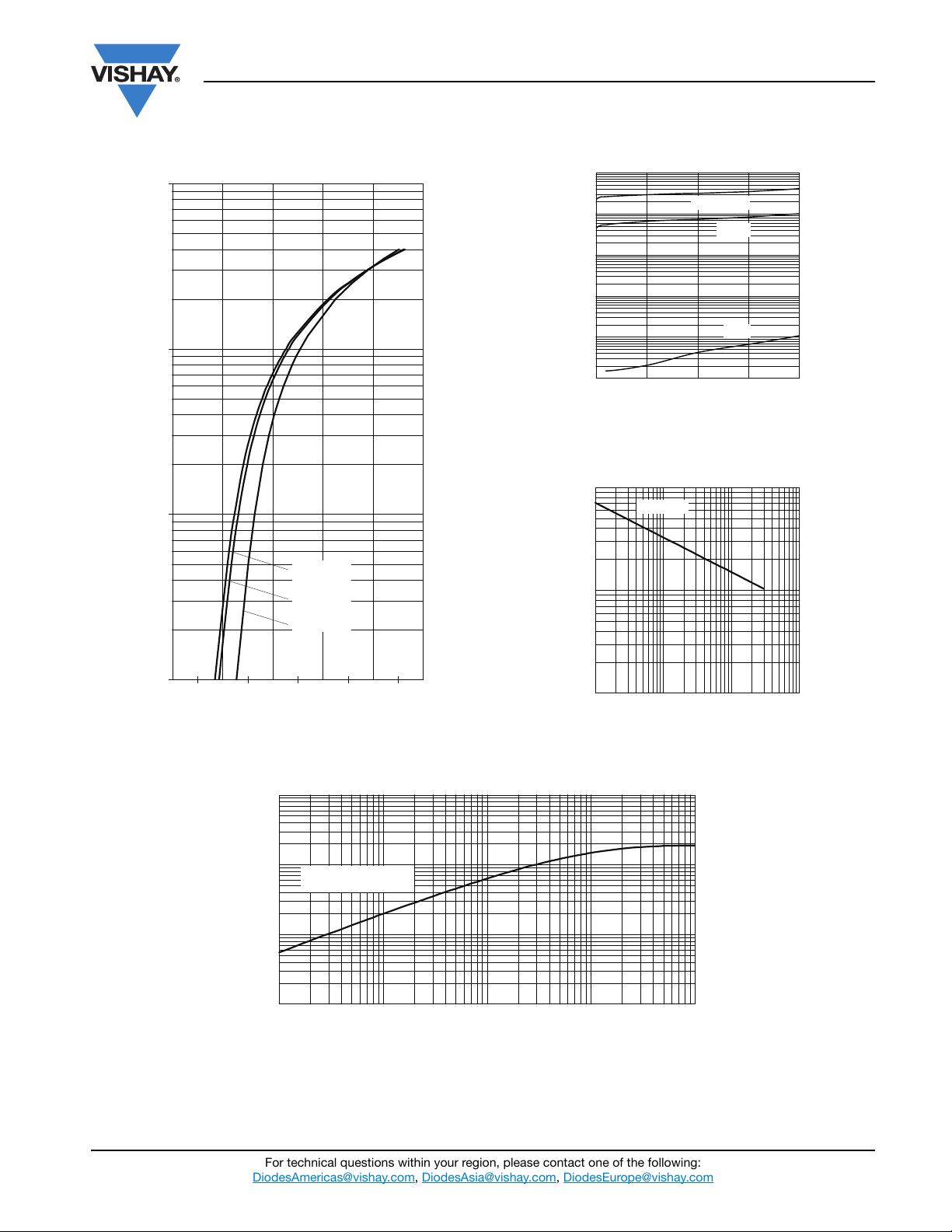
Forward Voltage Drop - VFM (V)
Instantaneous Forward Current - I
F
(A)
1
10
100
1000
0 0.5 1 1.5 2 2.5
Tj = 150˚C
Tj = 125˚C
Tj = 25˚C
Reverse Voltage - V (V)
Junction Capacitance - C
T
( p F )
10
100
1000
1 10 100 1000
Tj = 25˚C
UFB60FA20P
Insulated Ultrafast
Rectifier Module, 60 A
(µA)
R
Reverse Current - I
0.001
Vishay Semiconductors
100
10
1
0.1
0.01
0 50 100 150 200
Reverse Voltage - VR (V)
Fig. 2 - Typical Values of Reverse Current vs.
Tj = 150˚C
125˚C
25˚C
Reverse Voltage
Fig. 1 - Maximum Forward Voltage Drop Characteristics
Document Number: 94520 For technical questions within your region, please contact one of the following: www.vishay.com
Revision: 21-Jul-10 DiodesAmericas@vishay.com
(Per Diode)
10
(°C/W)
thJC
1
0.1
Thermal Impedance Z
0.01
0.0001 0.001 0.01 0.1 1
Single Pulse
(Thermal Resistance)
t1, Rectangular Pulse Duration (Seconds)
Fig. 4 - Maximum Thermal Impedance Z
, DiodesAsia@vishay.com, DiodesEurope@vishay.com 3
Fig. 3 - Typical Junction Capacitance vs. Reverse Voltage
Characteristics (Per Diode)
thJC
Page 4

UFB60FA20P
Average Forward Current - I
F(AV)
(A)
Allowable Case Temperature (°C)
80
90
100
110
120
130
140
150
0 5 10 15 20 25 30 35
DC
see note (1)
Square wave (D = 0.50)
Rated Vr applied
Average Power Loss ( W )
Average Forward Current - I
F(AV)
(A)
0
5
10
15
20
25
30
0 5 10 15 20 25 30 35
RMS Limit
D = 0.01
D = 0.05
D = 0.10
D = 0.20
D = 0.50
DC
trr ( ns )
dIF/dt (A/µs )
10
20
30
40
50
60
70
0001001
Tj = 125˚C
Tj = 25˚C
If = 30A
Vrr = 100V
Qrr ( nC )
dIF/dt (A/µs )
0
50
100
150
200
250
300
350
400
450
500
550
0001001
Tj = 125˚C
Tj = 25˚C
If = 30A
Vrr = 100V
Vishay Semiconductors
Fig. 5 - Maximum Allowable Case Temperature vs.
Average Forward Current (Per Leg)
Insulated Ultrafast
Rectifier Module, 60 A
Fig. 7 - Typical Reverse Recovery Time vs. dI
/dt
F
Fig. 6 - Forward Power Loss Characteristics (Per Leg)
Note
(1)
Formula used: TC = TJ - (Pd + Pd
Pd = Forward power loss = I
Pd
= Inverse power loss = VR1 x IR (1 - D); IR at VR1 = Rated V
REV
www.vishay.com For technical questions within your region, please contact one of the following: Document Number: 94520
4 DiodesAmericas@vishay.com
F(AV)
REV
x VFM at (I
) x R
;
thJC
/D) (see fig. 6);
F(AV)
Fig. 8 - Typical Stored Charge vs. dI
R
/dt
F
, DiodesAsia@vishay.com, DiodesEurope@vishay.com Revision: 21-Jul-10
Page 5

Q
rr
0.5 I
RRM
dI
(rec)M
/dt
0.75 I
RRM
I
RRM
t
rr
t
b
t
a
I
F
dIF/dt
0
(1)
(2)
(3)
(4)
(5)
(1) dI
F
/dt - rate of change of current
through zero crossing
(2) I
RRM
- peak reverse recovery current
(3) t
rr
- reverse recovery time measured
from zero crossing point of negative
going I
F
to point where a line passing
through 0.75 I
RRM
and 0.50 I
RRM
extrapolated to zero current.
(4) Q
rr
- area under curve dened by t
rr
and I
RRM
trr x I
RRM
2
Q
rr
=
(5) dI
(rec)M
/dt - peak rate of change of
current during t
b
portion of t
rr
UFB60FA20P
Insulated Ultrafast
Rectifier Module, 60 A
= 200 V
V
R
0.01 Ω
L = 70 μH
D.U.T.
dIF/dt
adjust
G
Fig. 9 - Reverse Recovery Parameter Test Circuit
D
IRFP250
S
Vishay Semiconductors
Document Number: 94520 For technical questions within your region, please contact one of the following: www.vishay.com
Revision: 21-Jul-10 DiodesAmericas@vishay.com
Fig. 10 - Reverse Recovery Waveform and Definitions
, DiodesAsia@vishay.com, DiodesEurope@vishay.com 5
Page 6

UFB60FA20P
Vishay Semiconductors
ORDERING INFORMATION TABLE
Device code
CIRCUIT CONFIGURATION
UF B 60 F A 20 P
1 - Ultrafast rectifier
2 - Ultrafast Pt diffused
3 - Current rating (60 = 60 A)
4 - Circuit configuration (2 separate diodes, parallel pin-out)
5 - Package indicator (SOT-227 standard isolated base)
6 - Voltage rating (20 = 200 V)
7
Insulated Ultrafast
Rectifier Module, 60 A
- P = Lead (Pb)-free
1
51324
4
67
2
LINKS TO RELATED DOCUMENTS
Dimensions www.vishay.com/doc?95036
Packaging information www.vishay.com/doc?95037
3
www.vishay.com For technical questions within your region, please contact one of the following: Document Number: 94520
6 DiodesAmericas@vishay.com
, DiodesAsia@vishay.com, DiodesEurope@vishay.com Revision: 21-Jul-10
Page 7

PACKAGING INFORMATION
Packaging Information
Vishay High Power Products
SOT-227
Tube
Quantities per tube is 10
M4 screw and washer included
Document Number: 95037 For technical questions concerning discrete products, contact: diodestech@vishay.com
Revision: 04-Jul-07 For technical questions concerning module products, contact: indmodules@vishay.com
www.vishay.com
1
Page 8

DIMENSIONS in millimeters (inches)
38.30 (1.508)
37.80 (1.488)
Ø 4.40 (0.173)
Ø 4.20 (0.165)
4 x M4 nuts
-A-
Outline Dimensions
Vishay High Power Products
SOT-227
Chamfer
2.00 (0.079) x 45°
4
12.50 (0.492)
12
7.50 (0.295)
30.20 (1.189)
29.80 (1.173)
2.10 (0.082)
1.90 (0.075)
8.10 (0.319)
4 x
7.70 (0.303)
Notes
• Dimensioning and tolerancing per ANSI Y14.5M-1982
• Controlling dimension: millimeter
3
6.25 (0.246)
15.00 (0.590)
2.10 (0.082)
1.90 (0.075)
25.70 (1.012)
25.20 (0.992)
R full
0.25 (0.010)
-C-
0.12 (0.005)
-B-
MMM
CA B
12.30 (0.484)
11.80 (0.464)
Document Number: 95036 For technical questions concerning discrete products, contact: diodes-tech@vishay.com
Revision: 28-Aug-07 For technical questions concerning module products, contact: ind-modules@vishay.com
www.vishay.com
1
Page 9

Legal Disclaimer Notice
Vishay
Disclaimer
All product specifications and data are subject to change without notice.
Vishay Intertechnology, Inc., its affiliates, agents, and employees, and all persons acting on its or their behalf
(collectively, “Vishay”), disclaim any and all liability for any errors, inaccuracies or incompleteness contained herein
or in any other disclosure relating to any product.
Vishay disclaims any and all liability arising out of the use or application of any product described herein or of any
information provided herein to the maximum extent permitted by law. The product specifications do not expand or
otherwise modify Vishay’s terms and conditions of purchase, including but not limited to the warranty expressed
therein, which apply to these products.
No license, express or implied, by estoppel or otherwise, to any intellectual property rights is granted by this
document or by any conduct of Vishay.
The products shown herein are not designed for use in medical, life-saving, or life-sustaining applications unless
otherwise expressly indicated. Customers using or selling Vishay products not expressly indicated for use in such
applications do so entirely at their own risk and agree to fully indemnify Vishay for any damages arising or resulting
from such use or sale. Please contact authorized Vishay personnel to obtain written terms and conditions regarding
products designed for such applications.
Product names and markings noted herein may be trademarks of their respective owners.
Document Number: 91000 www.vishay.com
Revision: 18-Jul-08 1
 Loading...