

Page 1
IR Receiver Modules for Remote Control Systems
4
3
2
1
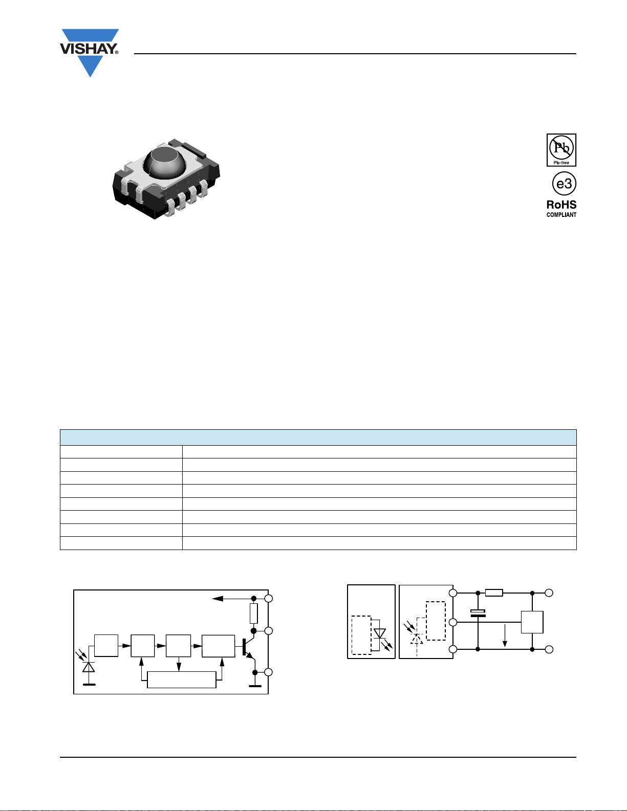
MECHANICAL DATA
Pinning
1 = GND, 2 = N.C., 3 = V
, 4 = OUT
S
DESCRIPTION
The TSOP61.. series are miniaturized SMD-IR receiver
modules for infrared remote control systems. PIN diode and
preamplifier are assembled on lead frame, the epoxy
package is designed as IR filter.
The demodulated output signal can directly be decoded by a
microprocessor. The main benefit is the operation with short
burst transmission codes and high data rates.
This component has not been qualified according to
automotive specifications.
16797
New TSOP61..
Vishay Semiconductors
FEATURES
• Photo detector and preamplifier in one package
• Internal filter for PCM frequency
• Continuous data transmission possible
• Supply voltage: 2.7 V to 5.5 V
• Output active low
• Low power consumption
• Compliant to RoHS directive 2002/95/EC and in
accordance to WEEE 2002/96/EC
SPECIAL FEATURES
• Enhanced data rate up to 4000 bit/s
• Operation with short burst possible (≥ 6 cycles/burst)
• Taping available for topview and sideview assembly
PARTS TABLE
CARRIER FREQUENCY SHORT BURSTS AND HIGH DATA RATES (AGC1)
30 kHz TSOP6130
33 kHz TSOP6133
36 kHz TSOP6136
36.7 kHz TSOP6137
38 kHz TSOP6138
40 kHz TSOP6140
56 kHz TSOP6156
BLOCK DIAGRAM APPLICATION CIRCUIT
17170_7
16838-1
PIN
Input
AGC
Band
pass
Control circuit
Demodulator
33 kΩ
3
V
S
4
OUT
1
GND
Transmitter
with
TSALxxxx
The external components R
to improve the robustnes against electrical overstress
(typical values are R
The output voltage V
below 1 V by the external circuit.
The capacitive load at the output should be less than 2 nF.
IR receiver
Circuit
and C1 are optional
1
= 100 Ω, C1 = 0.1 µF).
1
should not be pulled down to a level
O
V
S
OUT
GND
R
1
+ V
C
1
V
O
S
µC
GND
Document Number: 82176 www.vishay.com
Rev. 2.0, 21-Apr-09 1
Page 2
New TSOP61..
Vishay Semiconductors
IR Receiver Modules for
Remote Control Systems
ABSOLUTE MAXIMUM RATINGS
PARAMETER TEST CONDITION SYMBOL VALUE UNIT
Supply voltage (pin 3) V
Supply current (pin 3) I
Output voltage (pin 4) V
Voltage at output to supply V
Output current (pin 4) I
Junction temperature T
Storage temperature range T
Operating temperature range T
Power consumption T
Note
(1)
Stresses beyond those listed under “Absolute Maximum Ratings” may cause permanent damage to the device. This is a stress rating only
and functional operation of the device at these or any other conditions beyond those indicated in the operational sections of this specification
is not implied. Exposure to absolute maximum rating condtions for extended periods may affect the device reliability.
ELECTRICAL AND OPTICAL CHARACTERISTICS
PARAMETER TEST CONDITION SYMBOL MIN. TYP. MAX. UNIT
Supply current (pin 3)
Supply voltage V
E
I
v
OSL
Transmission distance
Output voltage low (pin 4)
Minimum irradiance
Maximum irradiance
Directivity Angle of half transmission distance ϕ
Note
(1)
T
= 25 °C, unless otherwise specified
amb
(1)
≤ 85 °C P
amb
E
= 0, VS = 5 V I
v
E
= 40 klx, sunlight I
v
= 0, test signal see fig. 1,
IR diode TSAL6200,
I
= 400 mA
F
= 0.5 mA, Ee = 0.7 mW/m2,
test signal see fig. 1
Pulse width tolerance:
- 5/fo < tpo < tpi + 6/fo,
t
pi
test signal see fig. 1
- 5/fo < tpo < tpi + 6/fo,
t
pi
test signal see fig. 1
- 0.3 to + 6.0 V
5mA
- 0.3 to 5.5 V
- 0.3 to (VS + 0.3) V
5mA
100 °C
- 40 to + 100 °C
- 25 to + 85 °C
10 mW
S
S
- V
O
stg
amb
tot
S
O
O
j
(1)
SD
SH
S
0.65 0.85 1.05 mA
0.95 mA
2.7 5.5 V
d40m
V
E
E
OSL
e min.
e max.
1/2
0.3 0.45 mW/m
30 W/m
± 50 deg
100 mV
2
2
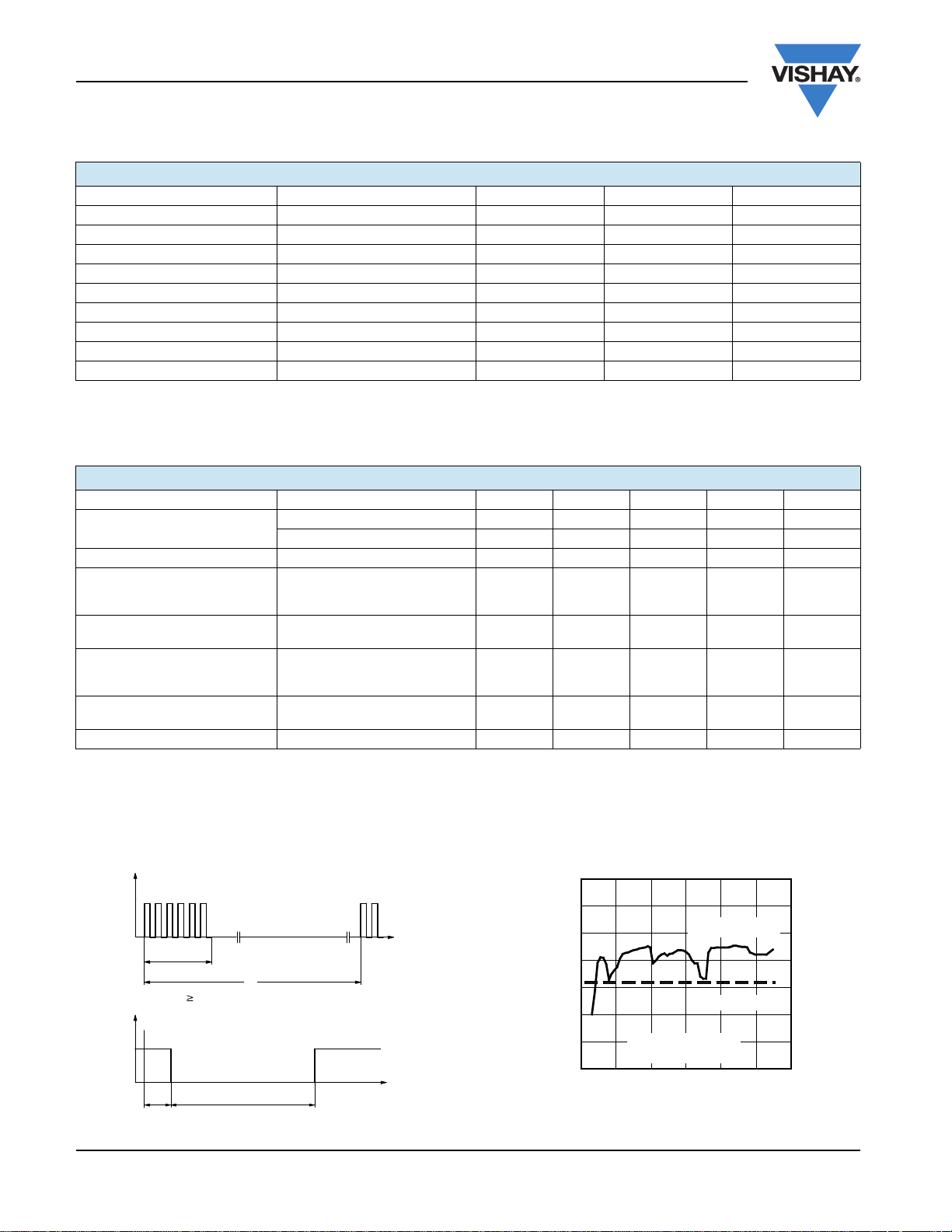
TYPICAL CHARACTERISTICS
T
= 25 °C, unless otherwise specified
amb
Optical Test Signal
E
e
(IR diode TSAL6200, IF = 0.4 A, N = 6 pulses,
*)
t
pi
*) tpi6/fo is recommended for optimal function
Output Signal
V
O
V
OH
V
OL
1)
3/f0 < td < 9/f
2)
tpi - 4/f0 < tpo < tpi + 6/f
1)
t
d
f = f
, t = 10 ms)
0
t
T
14337
0
2)
t
po
0
t
Fig. 1 - Output Active Low Fig. 2 - Pulse Length and Sensitivity in Dark Ambient
www.vishay.com Document Number: 82176
2 Rev. 2.0, 21-Apr-09
0.35
0.30
0.25
0.20
0.15
0.10
- Output Pulse Width (ms)
po
0.05
t
0
0.1 1 10 10
21391_1
λ = 950 nm,
Optical Test Signal, Fig.1
Ee - Irradiance (mW/m²)
Output Pulse Width
Input Burst Length
2103
10410
5
Page 3
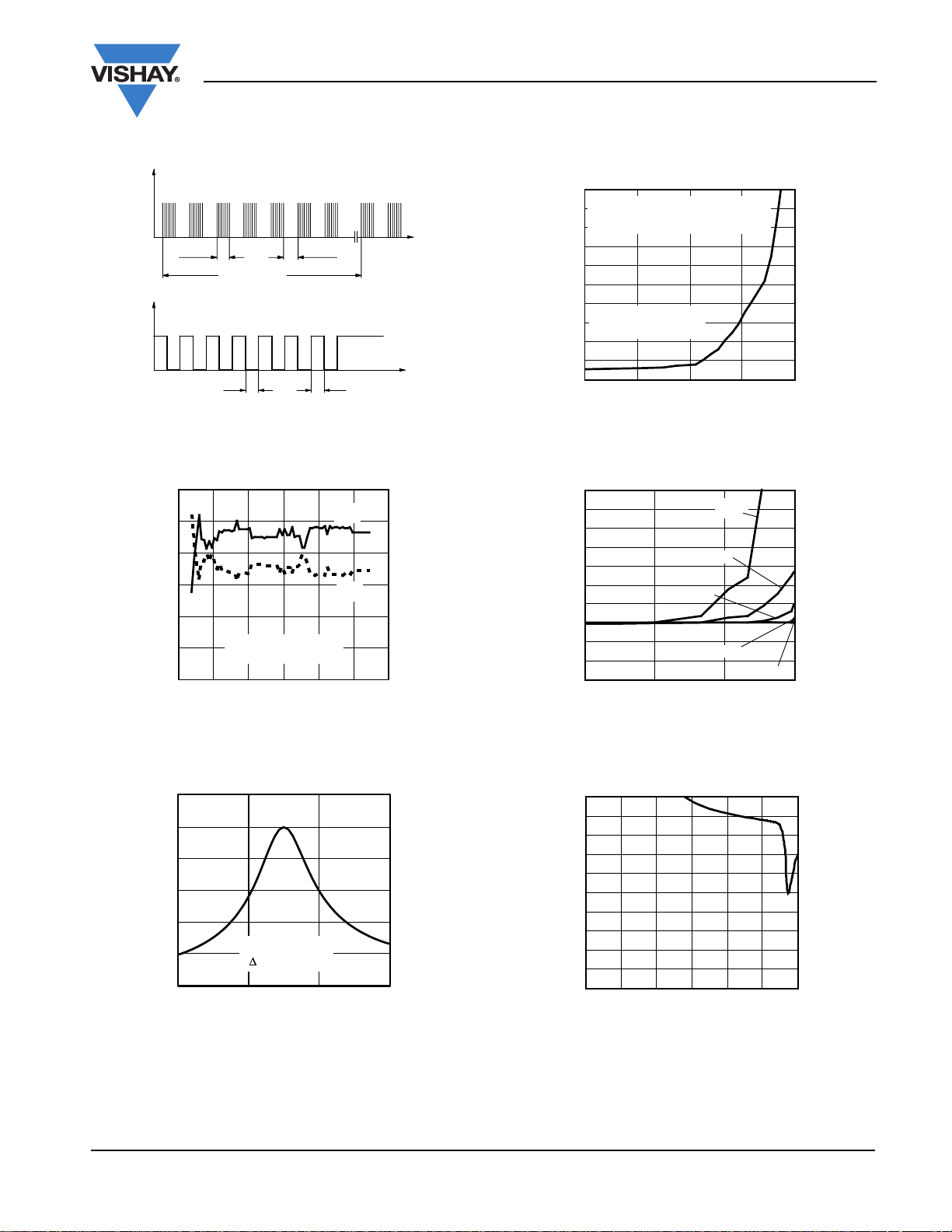
New TSOP61..
Optical Test Signal
E
e
600 µs 600 µs
t = 60 ms
Output Signal, (see fig. 4)
V
O
V
OH
V
OL
t
on
Fig. 3 - Output Function
0.8
0.7
0.6
0.5
0.4
- Output Pulse Width (ms)
off
0.3
, T
on
T
0.2
0.1 1 10 10
21392_1
Optical Test Signal, Fig. 3
Ee - Irradiance (mW/m²)
Fig. 4 - Output Pulse Diagram
λ = 950 nm,
2103
t
off
T
on
T
off
10410
IR Receiver Modules for
Remote Control Systems
t
94 8134
- Threshold Irradiance (mW/m²)
t
5
E
21393
- Threshold Irradiance (mW/m²)
E
21394
Vishay Semiconductors
5
Correlation with Ambient Light Sources:
4.5
10 W/m² = 1.4 kLx (Std. illum. A, T = 2855 K)
10 W/m² = 8.2 kLx (Daylight, T = 5900 K)
4
3.5
3
2.5
2
Wavelength of Ambient
1.5
Illumination: λ = 950 nm
1
0.5
e min.
0
0.01 0.1 1 10 100
Ee - Ambient DC Irradiance (W/m²)
Fig. 6 - Sensitivity in Bright Ambient
1
f = 30 kHz
f = f
0
f = 10 kHz
f = 100 Hz
0.9
0.8
0.7
0.6
0.5
0.4
0.3
0.2
0.1
e min.
0
1 10 100 1000
ΔVs
- AC Voltage on DC Supply Voltage (mV)
RMS
f = 20 kHz
Fig. 7 - Sensitivity vs. Supply Voltage Disturbances
1.2
1.0
8
0.
0.6
- Rel. Responsivity
e
0.4
/E
e min.
0.2
E
0.0
0.7 0.9 1.1 1.3
16926
f = f0 ± 5 %
f (3 dB) = f0/7
f/f0- Relative Frequency
Fig. 5 - Frequency Dependence of Responsivity
500
450
400
350
300
250
200
150
100
E - Max. Field Strength (V/m)
50
0
0 500 1000 1500 2000 2500 3000
20747
f - EMI Frequency (MHz)
Fig. 8 - Sensitivity vs. Electric Field Disturbances
Document Number: 82176 www.vishay.com
Rev. 2.0, 21-Apr-09 3
Page 4
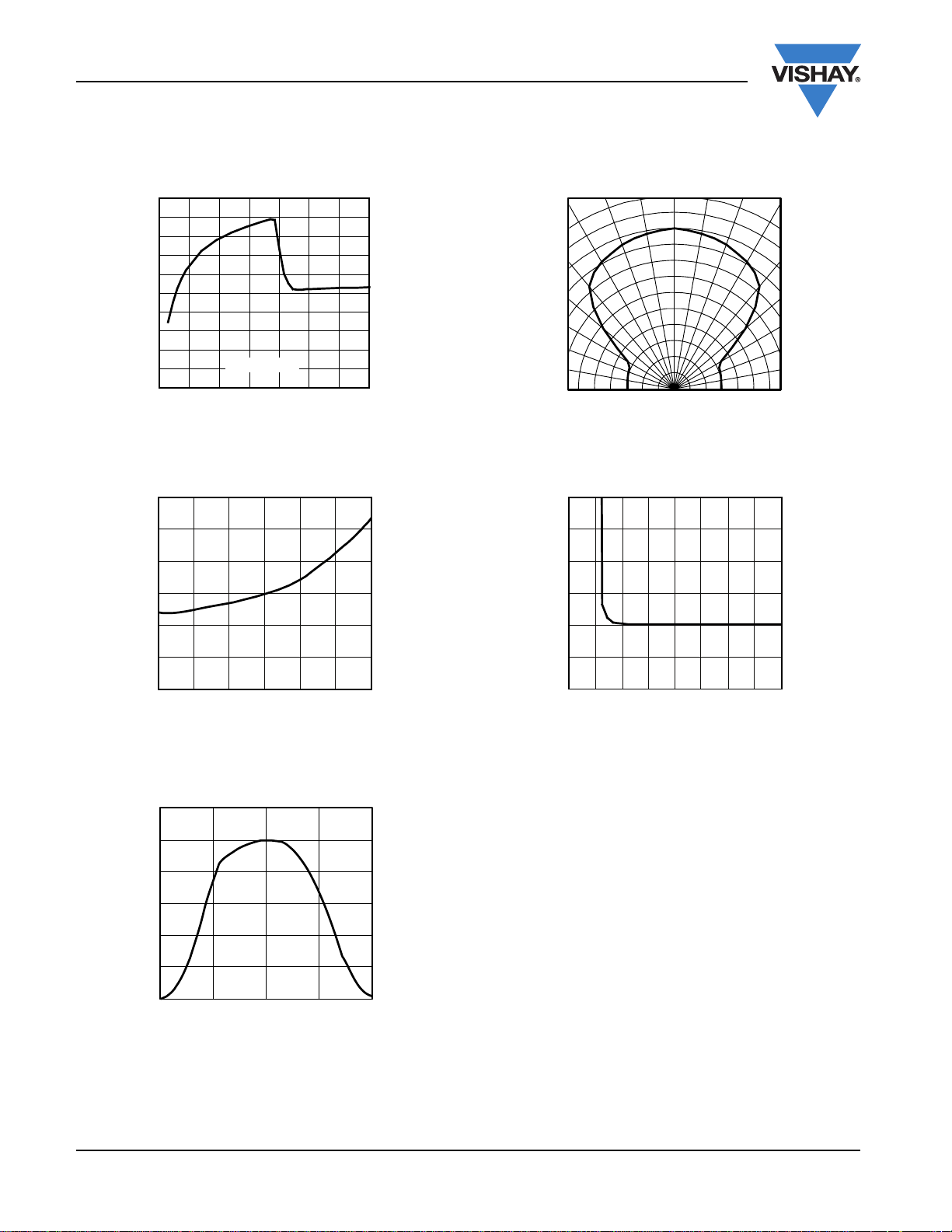
New TSOP61..
Vishay Semiconductors
1
0.9
0.8
0.7
0.6
0.5
0.4
0.3
0.2
Max. Envelope Duty Cycle
0.1
0
0 20 40 60 80 100 120
21396_1
Burst Length (number of cycles/burst)
Fig. 9 - Max. Envelope Duty Cycle vs. Burst Length
0.45
0.4
Ee = 2 mW/m²
IR Receiver Modules for
Remote Control Systems
1.0
0.9
0.8
0.7
140
16801
0.5
0.45
0°
0.4 0.2 0 0.2 0.4
0.6
d
- Relative Transmission Distance
rel
Fig. 12 - Horizontal Directivity
10° 20°
30°
40°
50°
60°
70°
80°
0.6
0.35
0.3
0.25
0.2
- Threshold Irradiance (mW/m²)
e min.
E
0.15
- 30 - 10 10 30 50 70 90
T
21397
- Ambient Temperature (°C)
amb
Fig. 10 - Sensitivity vs. Ambient Temperature
1.2
1.0
0.8
0.6
0.4
0.2
rel
S ( ) - Relative Spectral Sensitivityλ
0.0
750 850 950 1050 1150
16919
λ - Wavelength (nm)
0.4
0.35
0.3
- Sensitivity (mW/m²)
e min.
0.25
E
0.2
1.5 2.5 3.5 4.5 5.52345
21398
VS - Supply Voltage (V)
Fig. 13 - Sensitivity vs. Supply Voltage
Fig. 11 - Relative Spectral Sensitivity vs. Wavelength
www.vishay.com Document Number: 82176
4 Rev. 2.0, 21-Apr-09
Page 5

New TSOP61..
IR Receiver Modules for
Vishay Semiconductors
Remote Control Systems
SUITABLE DATA FORMAT
The TSOP61.. series is designed to suppress spurious
output pulses due to noise or disturbance signals. Data and
disturbance signals can be distinguished by the devices
according to carrier frequency, burst length and envelope
duty cycle. The data signal should be close to the band-pass
center frequency (e.g. 38 kHz) and fulfill the conditions in the
table below.
When a data signal is applied to the TSOP61.. in the
presence of a disturbance signal, the sensitivity of the
receiver is reduced to insure that no spurious pulses are
present at the output. Some examples of disturbance signals
which are suppressed are:
• DC light (e.g. from tungsten bulb or sunlight)
• Continuous signals at any frequency
• Modulated IR signals from common fluorescent lamps
(example of noise pattern is shown in figure 14)
Minimum burst length 6 cycles/burst
After each burst of length
a minimum gap time is required of
For bursts greater than
a minimum gap time in the data stream is needed of
Maximum number of continuous short bursts/second 2000
Recommended for NEC code yes
Recommended for RC5/RC6 code yes
Recommended for RCMM code yes
Recommended for RECS-80 code yes
Recommended for r-Step and r-Map data format yes
Recommended for XMP data format yes
Suppression of interference from fluorescent lamps Most common disturbance signals are suppressed
Note
For data formats with long bursts (10 carrier cycles or longer) we recommend the TSOP62.. because of the better noise suppression.
IR Signal
IR Signal from Fluorescent
Lamp with Low Modulation
0101520
16920
Fig. 14 - IR Signal from Fluorescent Lamp
5
Time (ms)
with Low Modulation
TSOP61..
6 to 70 cycles
≥ 10 cycles
70 cycles
> 1.1 x burst length
Document Number: 82176 www.vishay.com
Rev. 2.0, 21-Apr-09 5
Page 6

New TSOP61..
Vishay Semiconductors
PACKAGE DIMENSIONS
2.8
1
1.27
IR Receiver Modules for
Remote Control Systems
± 0.5
7.5
7.2
4
0.5
0.5
4x
3 x 1.27 = 3.81
5.51
0.5
Pick and place area. TT taping
A
5.3
(1.5)
0.1
0.1
A
(1.4)
± 0.5
2.9
4
Ø 2.2
Pick and place area. TR taping
2.6
2.35
R 1.7
Drawing-No.: 6.544-5341.01-4
Issue: 7; 23.03.09
16776
Not indicated tolerances ± 0.3
Footprint
3 x 1.27 = 3.81
1.27
0.9
technical drawings
according to DIN
specifications
2.2
ASSEMBLY INSTRUCTIONS
Reflow Soldering
• Reflow soldering must be done within 72 h while stored
under a max. temperature of 30 °C, 60 % RH after opening
the dry pack envelope
• Set the furnace temperatures for pre-heating and heating
in accordance with the reflow temperature profile as shown
in the diagram. Excercise extreme care to keep the
maximum temperature below 260 °C. The temperature
shown in the profile means the temperature at the device
surface. Since there is a temperature difference between
the component and the circuit board, it should be verified
that the temperature of the device is accurately being
measured
www.vishay.com Document Number: 82176
6 Rev. 2.0, 21-Apr-09
• Handling after reflow should be done only after the work
surface has been cooled off
Manual Soldering
• Use a soldering iron of 25 W or less. Adjust the
temperature of the soldering iron below 300 °C
• Finish soldering within 3 s
• Handle products only after the temperature has cooled off
Page 7

C
New TSOP61..
IR Receiver Modules for
Remote Control Systems
VISHAY LEAD (Pb)-FREE REFLOW SOLDER PROFILE
300
255 °C
250
240 °C
217 °C
200
150
T (°C)
100
50
0
0 50 100 150 200 250 300
19800
TAPING VERSION TSOP..TT dimensions in millimeters
max. 120 s
max. Ramp Up 3 °C/s
max. Ramp Down 6 °C/s
t (s)
Vishay Semiconductors
max. 260 °C
245 °
max. 20 s
max. 100 s
max. 2 cycles allowed
16584
Document Number: 82176 www.vishay.com
Rev. 2.0, 21-Apr-09 7
Page 8

New TSOP61..
Vishay Semiconductors
IR Receiver Modules for
Remote Control Systems
TAPING VERSION TSOP..TR dimensions in millimeters
16585
www.vishay.com Document Number: 82176
8 Rev. 2.0, 21-Apr-09
Page 9

New TSOP61..
REEL DIMENSIONS in millimeters
IR Receiver Modules for
Remote Control Systems
Vishay Semiconductors
16734
LEADER AND TRAILER dimensions in millimeters
Trailer Leader
no devices
min.
200
COVER TAPE PEEL STRENGTH
According to DIN EN 60286-3
0.1 N to 1.3 N
300 ± 10 mm/min.
165° to 180° peel angle
Document Number: 82176 www.vishay.com
Rev. 2.0, 21-Apr-09 9
devices
no devices
StartEnd
min. 400
96 11818
LABEL
Standard bar code labels for finished goods
The standard bar code labels are product labels and used for
identification of goods. The finished goods are packed in final
packing area. The standard packing units are labeled with
standard bar code labels before transported as finished
goods to warehouses. The labels are on each packing unit
and contain Vishay Semiconductor GmbH specific data.
Page 10

New TSOP61..
Vishay Semiconductors
IR Receiver Modules for
Remote Control Systems
VISHAY SEMICONDUCTOR GMBH STANDARD BAR CODE PRODUCT LABEL (Finished Goods)
PLAIN WRITING ABBREVIATION LENGTH
Item-description - 18
Item-number INO 8
Selection-code SEL 3
LOT-/serial-number BATCH 10
Data-code COD 3 (YWW)
Plant-code PTC 2
Quantity QTY 8
Accepted by ACC -
Packed by PCK -
Mixed code indicator MIXED CODE -
Origin xxxxxxx+ Company logo
LONG BAR CODE TOP TYPE LENGTH
Item-number N 8
Plant-code N 2
Sequence-number X 3
Quantity N 8
Total length - 21
SHORT BAR CODE BOTTOM TYPE LENGTH
Selection-code X 3
Data-code N 3
Batch-number X 10
Filter - 1
Total length - 17
DRY PACKING
The reel is packed in an anti-humidity bag to protect the
devices from absorbing moisture during transportation and
storage.
Aluminum bag
After more than 72 h under these conditions moisture
content will be too high for reflow soldering.
In case of moisture absorption, the devices will recover to the
former condition by drying under the following condition:
192 h at 40 °C + 5 °C/ - 0 °C and < 5 % RH (dry air/nitrogen)
or
96 h at 60 °C + 5 °C and < 5 % RH for all device containers or
Label
24 h at 125 °C + 5 °C not suitable for reel or tubes.
An EIA JEDEC standard JESD22-A112 level 4 label is
included on all dry bags.
Reel
15973
FINAL PACKING
The sealed reel is packed into a cardboard box. A secondary
cardboard box is used for shipping purposes.
RECOMMENDED METHOD OF STORAGE
Dry box storage is recommended as soon as the aluminum
bag has been opened to prevent moisture absorption. The
following conditions should be observed, if dry boxes are not
available:
• Storage temperature 10 °C to 30 °C
• Storage humidity ≤ 60 % RH max.
www.vishay.com Document Number: 82176
10 Rev. 2.0, 21-Apr-09
Example of JESD22-A112 level 4 label
Page 11

New TSOP61..
IR Receiver Modules for
Remote Control Systems
ESD PRECAUTION
Proper storage and handling procedures should be followed
to prevent ESD damage to the devices especially when they
are removed from the antistatic shielding bag. Electro-static
sensitive devices warning labels are on the packaging.
Vishay Semiconductors
VISHAY SEMICONDUCTORS STANDARD
BAR CODE LABELS
The Vishay Semiconductors standard bar code labels are
printed at final packing areas. The labels are on each
packing unit and contain Vishay Semiconductors specific
data.
16962
Document Number: 82176 www.vishay.com
Rev. 2.0, 21-Apr-09 11
Page 12

Legal Disclaimer Notice
Vishay
Disclaimer
All product specifications and data are subject to change without notice.
Vishay Intertechnology, Inc., its affiliates, agents, and employees, and all persons acting on its or their behalf
(collectively, “Vishay”), disclaim any and all liability for any errors, inaccuracies or incompleteness contained herein
or in any other disclosure relating to any product.
Vishay disclaims any and all liability arising out of the use or application of any product described herein or of any
information provided herein to the maximum extent permitted by law. The product specifications do not expand or
otherwise modify Vishay’s terms and conditions of purchase, including but not limited to the warranty expressed
therein, which apply to these products.
No license, express or implied, by estoppel or otherwise, to any intellectual property rights is granted by this
document or by any conduct of Vishay.
The products shown herein are not designed for use in medical, life-saving, or life-sustaining applications unless
otherwise expressly indicated. Customers using or selling Vishay products not expressly indicated for use in such
applications do so entirely at their own risk and agree to fully indemnify Vishay for any damages arising or resulting
from such use or sale. Please contact authorized Vishay personnel to obtain written terms and conditions regarding
products designed for such applications.
Product names and markings noted herein may be trademarks of their respective owners.
Document Number: 91000 www.vishay.com
Revision: 18-Jul-08 1
 Loading...