

Page 1

SIR Endec for IrDA Applications
Integrated Interface Circuit
Description
The TOIM4232 Endec IC provides proper pulse shaping for the SIR IrDA
as of the 4000-series. For transmitting the TOIM4232
shortens the RS232 output signal to IrDA compatible
electrical pulses to drive the infrared transmitter. In
the receive mode, the TOIM4232 stretches the
received infrared pulses to the proper bit width
depending on the operating bit rate. The IrDA bit rate
varies from 2.4 kbit/s to 115.2 kbit/s.The TOIM4232 is
using a crystal clock 3.6864 MHz for its pulse stretching and shortening. The clock can be generated by
the internal oscillator. An external clock can be used,
too. The TOIM4232 is programmable to operate from
1200 bit/s to 115.2 kbit/s by the communication software through the RS232 port. The output pulses are
software programmable as either 1.627 µs or 3/16 of
bit time. The typical power consumption is very low
with about 10 mW in operational state and in the order
of a few microwatts in standby mode.
ULC Technology: High performance gate array
package using multiple metal layer CMOS technology
featuring sub-micron channel lengths (0.35 µm).
®
front end infrared transceivers
TOIM4232
Vishay Semiconductors
18080
Features
• Pulse shaping function (shortening
and stretching) used in SIR IrDA
applications
• Directly interfaces the SIR transceiver
TFD..- and TFB..- series to an RS232 port
• Programmable baud clock generator (1200 Hz to
115.2 kHz), 13 baud rates
• 3/16 bit pulse duration or 1.627 µs pulse selectable
• SO16 - package
• 2.7 V to 3.6 V operation voltage, 5 V tolerant inputs
• Low operating current
• Lead (Pb)-free device
• Device in accordance to RoHS 2002/95/EC and
WEEE 2002/96EC
®
e3
Ordering Information
Part Number Qty / Reel
TOIM4232-TR1 500 pcs
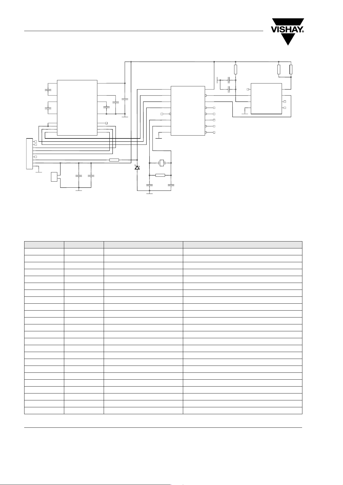
Block Diagram
Document Number 82546
Rev. 1.4, 07-Dec-05
TD_232
RD_232
BR/D
RESET
GND
Vcc
Endec
Baud
Generator
Logic
Osci llator
X1
TD_IR
RD_IR
TD_LED
RD_LED
S1
S2
Vcc_SD
X2
18079
www.vishay.com
1
Page 2

TOIM4232
Vishay Semiconductors
Pin Assignment and Description
Pin Number Symbol Description I/O Active
1 RESET Resets all internal registers. Initially must be HIGH ("1") to reset internal
registers. When HIGH, the TOIM4232 sets the IrDA default bit rate of 9600
bit/s, sets pulse width to 1.627 µs. The V
reset signal which allows to shut down of a TFDx4x00 transceiver when
applying the reset signal to the TOIM4232. When using devices with
external SD like TFDS4203, the reset line can be used directly as shut
down signal. RESET pin can be controlled by either the RTS or DTR line
through RS232 level converter. Minimum hold time for resetting is 1 µs.
Disables the oscillator when active.
2BR/ D Baud Rate control/ Data.
BR/ D = 0, data communication mode:
RS232 TXD data line is connected (via a level shifter) to TD_232 input pin.
The TXD - signal is appropriately shortened and applied to the output
TD_IR, driving the TXD input of the IR transceiver. The RXD line of the
transceiver is connected to the RD_IR input. This signal is stretched to the
correct bit length according the programmed bit rate and is routed to the
RS232 RXD line at the RD_232 pin.
Data received from the RS232 port is interpreted as Control Word. The
Control Word programs the baud rate width will be effective as soon as BR/
3 RD_232 Received signal data output of stretched signal to the RS232 RXD line
4 TD_232 Input of the signal to be transmitted from the RS232 port TXD line (passing
5V
6 X1 Crystal input clock, 3.6864 MHz nominal. Input for external clock *) I
7X2 Crystal *) I
8 GND Ground in common with the RS232 port and IrDA transceiver ground
9 TD_LED Transmit LED indicator driver. Use 180 Ω current limiting resistor in.series
10 RD_LED Receive LED indicator driver. Use 180 Ω current limiting resistor in series
11 NC No connection
12 S1 User Programmable Bit. Can be used to turn ON/ OFF a front-end infrared
13 S2 User Programmable Bit. Can be used to turn ON/ OFF a front-end infrared
14 TD_IR Data output of shortened signal to the infrared transceiver O HIGH
15 RD_IR Data input from the infrared transceiver, min. pulse duration 1.63 µs **) I LOW
16 VCC Supply voltage I
*) Crystal should be connected as shown in figure 2. In addition connect a 100 kΩ resistor from Pin 6 to Pin 7 and from Pin 6 and Pin 7 a
22 pF capacitor to ground, respectively. When an external clock is available connect it to Pin 6 leaving Pin 7 open. The external resistor
of 100 kΩ is used to accelerate the start of oscillation after reset or power - on. The value depends on the "Q" of the resonator. With low
Q resonators it is not necessary. The start - up time of the oscillator is between 30 µs (with piezo resonators) and above 2 ms with high Q
quartzes.
**) All Vishay Semiconductor SIR transceivers fulfill this condition
_SD Outputs an inverted RESET signal. Can be used to shut down the power
CC
supply of a 4000 series transceiver (e.g., TFDU4100). V
output function. This pin can be used to shut down a transceiver (e.g.,
TFDx4xxx). Output polarity: Inverted RESET input.
transceiver (e.g., an infrared module at the adapter front)
transceiver (e.g., an infrared module at the adapter back)
BR/ D = 1, Programming mode:
D return to LOW.
(using level converter).
the level converter).
to LED to connect to V
to LED to connect to V
_SD output is simply an inverted
CC
shutdown
CC
. (VCC = 3.3 V)
CC
. (VCC = 3.3 V)
CC
OHIGH
IHIGH
OLOW
OLOW
OLOW
OLOW
OLOW
HIGH
www.vishay.com
2
Document Number 82546
Rev. 1.4, 07-Dec-05
Page 3

TOIM4232
Vishay Semiconductors
Block diagram of application circuit
Operating the interface circuit at a PC COM - port.
When operating directly with an UART with 3 V - or
5 V - logic, in the application circuit no level converter
is necessary.
DTR
RTS
TXD
RXD
RS232 9 pin
connector
18081
Level
converter
RESET VCC_SD
BR/D TD_IR
TD_232 RD_IR
RD_232
TOIM4232
X1
C1
R1
100 kΩ
3.6864 MHz
2x22pF
VCC
TXD
RXD
TFDU4100
X2
TFDS420x
TFDU4300
C2
Table 1.
Recommended Application Circuit Components
Component Recommended Value Vishay Part Number
C1 22 pF VJ 1206 A 220 J XAMT
C2 22 pF VJ 1206 A 220 J XAMT
R1 100 kΩ CRCW-1206-1003-F-RT1
Quartz Crystal 3.686400 MHz XT49S - 20 - 3.686400M
Absolute Maximum Ratings
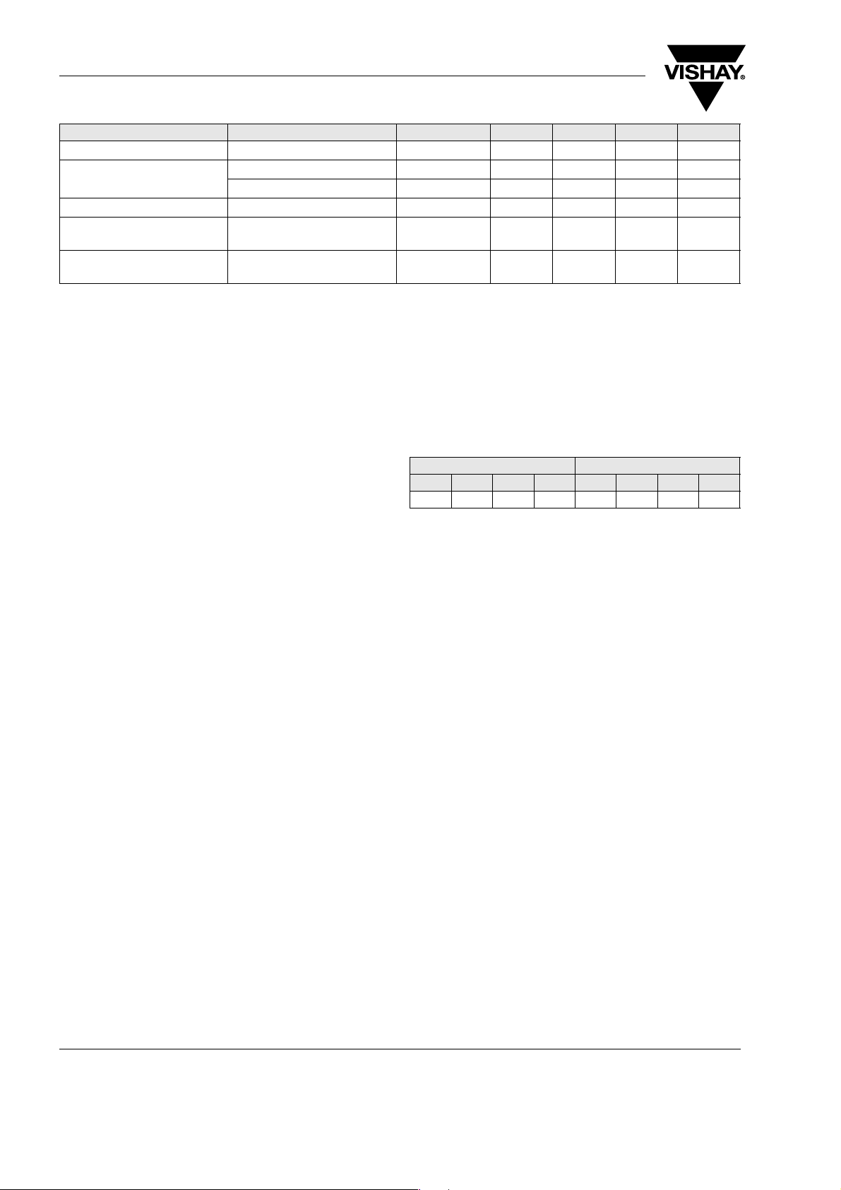
Parameter Test Conditions Symbol Min Ty p. Max Unit
Supply voltage V
CC
- 0.5 3.6 V
Input voltage all pins - 0.5 5.5 V
Output voltage all pins - 0.5 V
Output sinking current, max all pins I
Junction temperature, max T
Ambient temperature
(operating)
Storage temperature T
Soldering temperature T
O
J
T
amb
stg
sldr
- 25 85 °C
- 25 85 °C
+ 0.5 V
CC
8mA
125 °C
260 °C
DC Characteristics
Parameter Test Conditions Symbol Min Ty p. Max Unit
Operating voltage V
VCC = 3.3 V ± 5 %, operating temperature = - 55 °C to + 125 °C
Parameter Test Conditions Symbol Min Ty p. Max Unit
Input HIGH voltage inputs tolerate levels as high as
5.5 V max. all inputs are Schmitt
trigger inputs
Input LOW voltage V
Input Schmitt trigger hysteresis V
V
CC
IH
IL
hyst
2.7 3.3 3.6 V
1.7 2.0 V
0.8 1.1 V
0.6 V
Document Number 82546
Rev. 1.4, 07-Dec-05
www.vishay.com
3
Page 4
TOIM4232
Vishay Semiconductors
Parameter Test Conditions Symbol Min Ty p. Max Unit
Input leakage no pull-up/down VIN = VDD or GND I
Output HIGH voltage I
Output LOW voltage I
Consumption current standby inputs grounded, no output load
Consumption current dynamic inputs grounded, no output load
= - 2.0 mA V
OH
I
= - 0.5 mA V
OH
= + 2.0 mA V
OL
V
= 3.3 V, T = 25 °C
CC
V
= 3.3 V, T = 25 °C
CC
L
OH
OH
OL
I
SB
I
CC
- 10 ± 1 10 µA
2.0 V
2.4 V
0.4 V
1µA
2mA
Operation Description
Figure 2 shows a typical example of an RS232 port
interface. The TOIM4232 connects to an RS232 level
converter on one side, and an infrared transceiver on
the other. The internal TOIM4232 baud rate generator
can be software controlled.
When BR/D = 0, the TOIM4232 interprets the channels TD_232 to TD_IR and RD_IR to RD_232 as data
channels.
On the other hand, whenever BR/D = 1, the
TOIM4232 interprets TD_232 as Control Word for
setting the Baud rate. The Baud rate can be programmed to operate from 1200 bit/s to 115.2 kbit/s.
As RS232 level converter, EIA232 or MAX232 or
equivalent are recommended.
When using the TOIM4232 directly connected to an
UART it is compatible to 5 V TTL and 3.3 V CMOS
logic.
Typical external resistors and capacitors are needed
as shown in the TFDx4xxx references.
The output pulse duration can also be programmed,
see chapter "Operation Description". It is strongly recommended using 1.627 µs output pulses to save battery power. As frequency determining component a
Vishay XT49M Crystal is recommended, when no
external clock is available.
We strongly recommend not to use this 3/16 mode
because 3/16 pulse length at lower bit rates consumes more power than the shorter pulse. At a
data rate of 9600 bit/s, the ratio of power consumption of both modes is a factor of 12 (!).
In this case the TOIM4232 interprets the 7 LSBs at
the TD_232 input as a Control Word. The operating
baud rate will change to its supposedly new baud rate
when the BR/D returns back to LOW ("0") Set the
UART to 8 bit, no parity, 1 stop bit.
Control Byte (8 bit)
First Character Second Character
X S2 S1 S0 B3 B2 B1 B0
LSB
X: Do not care
S1, S2: User programmble bit to program the outputs
S1 and S2
S0: Irda pulse select
S0 = (1): 1.627 µs pulses
S0 = (0): 3/16 bit time pulses, not recommended
B0 .. B3: Baud rate select words
Example:
To set TOIM4232 at COM2 port (2F8) to 9600 bit/s
with 3/16 bit time pulse duration send to the
TOIM4232 in programming mode in e.g. "Basic"
OUT &H2F8, (&H6)
For same port, 9600 bit/s and 1.627 µs pulse duration
send
OUT &H2F8, (&H16)
For additionally activating S1 send
OUT &H2F8, (&H36)
Programming the TOIM4232
For correct, data rate dependent timing the
TOIM4232 is using a built-in baud rate generator.
This is used when no external clock is not available as
in RS232 IR-dongle applications. For programming
the BR/D pin has to be set active, BR/D = 1.
www.vishay.com
4
Document Number 82546
Rev. 1.4, 07-Dec-05
Page 5

Baud Rate Select Words
B3 B2 B1 B0
00000 115.2 k
0011 57.6 k
0102 38.4 k
0113 19.2 k
1004 14.4 k
1015 12.8 k
1106 9.6 k
1117 7.2 k
10008 4.8 k
0019 3.6 k
010A 2.4 k
011B 1.8 k
100C 1.2 k
101D forbidden
110E forbidden
111F forbidden
Note: IrDA standard only supports 2.4, 9.6, 19.2, 57.6, and 115.2 kbit/s.
2nd
Char
Baud Rate
TOIM4232
Vishay Semiconductors
Software for the TOIM4232
UART Programming
For proper operation, the RS232 must be programmed (using 8 bit, 1 stop, no parity) to send a two character control word, YZ. The control
word YZ is composed of two characters, written in hexadecimal, in format: YZ. The transfer rate for programming must be identical with
the formerly programmed data rate, or after resetting the TOIM4232, the default rate of 9600 bit/s is used.
Step. RESET BR/ D TD_UART RD_UART RD_IR TD_IR Description and Comments
1HighXXXXXResets all internal registers. Resets to
2LowXXXXXWait at least 2 ms, to allow start-up of
3LowHighXXXXWait at least 7 µs. TOIM4232 now is set
4LowHighYZ
with Y = 1
for 1.627 µs
Y = 0
3/16 bit
length
5 Low Low DATA DATA DATA DATA With BR/D = 0, TOIM4232 is in the data
*) For programming the UART, refer to e.g., National Semiconductor’s data sheet of PC 16550 UART
X X X Sending the Control Word YZ.
IrDA default data rate of 9600 bit/s
internal clock. When external clock is
used: Wait at least 7 µs.
to the Control Word programming mode
Examples: Send "1Z" if 1.627 µs pulses
are intended to be used. Otherwise
send "0Z" for 3/16 bit period pulses.
"Y6" keeps the 9.6 kbit/s data rate.
Z = 0 sets to 115.2 kbit/s, see
programming table.
Wait at least 1 µs for hold-time.
communication mode. Both RESET
and BR/D must be kept LOW ("0")
during data transmission.
Reprogramming to a new data rate can
be resumed by restarting from step 3.
The UART itself also must set to the
correct data rate *).
Document Number 82546
Rev. 1.4, 07-Dec-05
www.vishay.com
5
Page 6
TOIM4232
Vishay Semiconductors
MAX3232CSE
1
J1
CON9
1
6
2
7
3
8
4
9
5
ext.
inputmax
3.3 V DC
+
C3
+
C4
11
10
12
RXD
RTS (BR/D)
TXD
DTR (Reset)
VCC
J2
CON2
C+
3
C1-
4
C2+
5
C2-
T1IN
T2IN
R1OUT
9
R2OUT
1
2
U1
VCC
V+
V-
GND
T1OUT
T2OUT
R1IN
R2IN
+
C1
C2
VCC
R6
Anode
TXD
R4
1
3
5
NC
R3
16
2
6
C6
+
15
14
7
13
8
C7
C5
+
+
R1
Z2
C8
TOIMx232
1
Reset
2
3
4
5
6
7
8 9
Y1
R2
U2
BR/Data
RD 232
TD 232
Vcc SD
X1
X2
GNDTDLED
C9
Vcc
RD IR
TD IR
S2
S1
NC
RD LED
Application circuit using TFDU4100 with integrated
level shifter MAX3232E. When used directly with
3 V
, this one can be omitted
logic
C11
C10
16
15
14
13
12
11
10
TFDU4100
+
IRED IRED
2
Cathode
4
RXD
U4
6
VCC1
8 7
GNDSC
Table 1.
Recommended Application Circuit Components
Component Recommended Value Vishay Part Number
1 C1 100 nF VJ 1206 Y 104 J XXMT
2 C2 10 µF, 16 V 293D106X9016B2T
3 C3 100 nF VJ 1206 Y 104 J XXMT
4 C4 100 nF VJ 1206 Y 104 J XXMT
5 C5 100 nF VJ 1206 Y 104 J XXMT
6 C6 100 nF VJ 1206 Y 104 J XXMT
7 C7 1 µF. 16 V 293D105X9016A2T
8 C8 22 pF VJ 1206 A 220 J XAMT
9 C9 22 pF VJ 1206 A 220 J XAMT
10 C10 6.8 µF, 16 V 293D 685X9 016B 2T
11 C11 100 nF VJ 1206 Y 104 J XXMT
12 Z2 3.6 V BZT55C3V6
13 R1 5.6 Ω CRCW-1206-5601-F-RT1
14 R2 100 kΩ (up to 1 MΩ, or omitted) CRCW-1206-1003-F-RT1
15 R3 47 Ω CRCW-1206-47R0-F-RT1
16 R4 20 Ω CRCW-1206-20R0-F-RT1
17 R6 20 Ω CRCW-1206-20R0-F-RT1
18 Y1 3.686400 MHz XT49S - 20 - 3.686400M
19 U1 MAXIM MAX 3232E
20 U2 TOIM4232
21 U3 TFDU4100
22 J1 9 Pin - D - Sub Cannon
23 J2 Power connector
24 PCB VISHAY Dongle_4
16527
www.vishay.com
6
Document Number 82546
Rev. 1.4, 07-Dec-05
Page 7

J1
opt.
1
6
2
7
3
8
4
9
5
CON9
18240
MAX3232CSE
1
C+
+
C3
3
C1-
4
C2+
+
C4
5
C2-
11
T1IN
10
T2IN
12
R1OUT
9
R2OUT
RXD
DTS (BR/D)
TXD
DTS (Reset)
VCC
J2
1
ext.
2
inputmax
CON2
3,6V DC
U1
VCC
GND
T1OUT
T2OUT
R1IN
R2IN
TOIM4232
Vishay Semiconductors
R4R3
16
2
V+
6
V-
+
15
14
7
13
8
+
C2C1
C7
C5
+
+
C6
R1
Z2
TOIMx232
1
Reset
2
BR/Data
3
RD 232
4
TD 232
5
Vcc SD
6
X1
7
X2
8 9
GNDTDLED
Y1
R2
C8 C9
U2
RD IR
TD IR
RD LED
15
14
13
S2
12
S1
11
NC
10
16
Vcc
Application circuit using TFDU4300 with an integrated
level shifter MAX3232E. When used directly with
3 V
, this one can be omitted
logic
C11
C10
TFDU4300
2
Cathode
4
RXD
6
VCC1
8 7
GND Vlog
U4
Anode
TXD
SD
1
3
5
Table 2.
Recommended Application Circuit Components
Component Recommended Value Vishay Part Number
1 C1 100 nF VJ 1206 Y 104 J XXMT
2 C2 10 µF, 16 V 293D106X9016B2T
3 C3 100 nF VJ 1206 Y 104 J XXMT
4 C4 100 nF VJ 1206 Y 104 J XXMT
5 C5 100 nF VJ 1206 Y 104 J XXMT
6 C6 100 nF VJ 1206 Y 104 J XXMT
7 C7 1 µF, 16 V 293D105X9016A2T
8 C8 22 pF VJ 1206 A 220 J XAMT
9 C9 22 pF VJ 1206 A 220 J XAMT
10 C10 6.8 µF, 16 V 293D 685X9 016B 2T
11 C11 100 nF VJ 1206 Y 104 J XXMT
12 Z2 3.6 V BZT55C3V6
13 R1 5.6 kΩ CRCW-1206-5601-F-RT1
14 R2 100 kΩ (up to 1 MΩ, or omitted) CRCW-1206-1003-F-RT1
15 R3 47 Ω CRCW-1206-47R0-F-RT1
16 R4 20 Ω CRCW-1206-20R0-F-RT1
17 Y1 3.686400 MHz XT49S - 20 - 3.686400M
18 U1 MAXIM MAX 3232E
19 U2 TOIM4232
20 U3 TFDU4300
21 J1 9 Pin - D-Sub Cannon
22 J2 Power connector
23 PCB VISHAY Dongle_4
Document Number 82546
Rev. 1.4, 07-Dec-05
www.vishay.com
7
Page 8

TOIM4232
Vishay Semiconductors
3
+
C1
R13
1
Q4
Vcc
2
+
Q2
C2
R2
+3,3V
R6
VB1
SUB-D 9
1
3
Q1
Vcc
1
2
D1
R9
R12/1
R3
D2
D4
1
6
2
7
3
8
4
9
5
TD232
D6D5
D7
3
RXD
RTS
TXD
DTR
Reset
BR/DRD232
R5 R1
+3.3 V
3
Q3
1
2
D3
RXD
RTS
TXD
R20
Reset
3
1
Q1
2
U1TOIM4232
Vcc
RD IR
TD IR
NC
RD LED
16
15
14
13
S2
12
S1
11
10
R10
C3
QZ1
1
Reset
2
BR/Data
3
RD 232
4
TD 232
5
Vcc SD
6
X1
7
X2
8 9
GNDTDLED
C4
Install Jumper connection only when VCC SD supplies
U2. In that case leave R11 off.
www.vishay.com
8
Jumper
R11
R12/2
2
4
RXD
6
Vcc
8
Gnd
+
C6
C5
U2 TFDU4100
IRED1
TXD
NC
SC
1
3
5
7
18082
IRED anodeIRED cathode
Document Number 82546
Rev. 1.4, 07-Dec-05
Page 9

Vishay Semiconductors
Table 3.
Recommended Application Circuit Components
Component Recommended Value Vishay Part Number
1 C1 22 µF, 16 V 293D 226X9 016C 2T
2 C2 47 µF, 16 V 293D 476X9 016D 2T
3 C3 22 pF VJ 1206 A 220 J XAMT
4 C4 22 pF VJ 1206 A 220 J XAMT
5 C5 100 nF VJ 1206 Y 104 J XXMT
6 C6 6.8 µF, 16 V 293D 685X9 016B 2T
7D1 1N4148
8D2 1N4148
9 D4 BZT55C4V7
10 D5 1N4148
11 D6 1N4145
12 D7 BZT55C3V9
13 IRED1 TSHF5400
14 Jumper CRCW-1206-000-F-RT1
15 LED1 TLLY4401
16 LED2 TLLG4401
17 Q1 BC817-25
18 Q2 VP 0610 0T
19 Q3 BC817-25
20 Q4 BC817-25
21 QZ1 3.686400 MHz XT49S - 20 - 3.686400M
22 R1 22 kΩ CRCW-1206-2202-F-RT1
23 R2 10 kΩ CRCW-1206-1002-F-RT1
24 R3 22 kΩ CRCW-1206-2202-F-RT1
25 R5 1 kΩ CRCW-1206-1001-F-RT1
26 R6 47 kΩ CRCW-1206-4702-F-RT1
27 R9 5.6 kΩ CRCW-1206-5601-F-RT1
28 R10 100 kΩ CRCW-1206-1003-F-RT1
29 R11 100 Ω CRCW-1206-1000-F-RT1
30 R12 20 Ω CRCW-1206-20R0-F-RT1
21 R13 1 kΩ CRCW-1206-1001-F-RT1
32 R17 750 Ω CRCW-1206-7500-F-RT1
33 R18 750 Ω CRCW-1206-750-F-RT1
34 VB1 9 Pin - D- Sub Cannon
35 PCB VISHAY Dongle_3
36 U1 TOIM4232
37 U2 TFDU4100
TOIM4232
Document Number 82546
Rev. 1.4, 07-Dec-05
www.vishay.com
9
Page 10
TOIM4232
Vishay Semiconductors
Package Dimensions in mm
Package SO16L
1.27
16 9
18
0.49
0.35
10.5
10.1
8.89
0.25
0.10
2.45
2.25
9.25
8.75
7.5
7.3
10.56
10.15
technical drawings
according to DIN
specifications
0.3
0.2
13011
www.vishay.com
10
Document Number 82546
Rev. 1.4, 07-Dec-05
Page 11

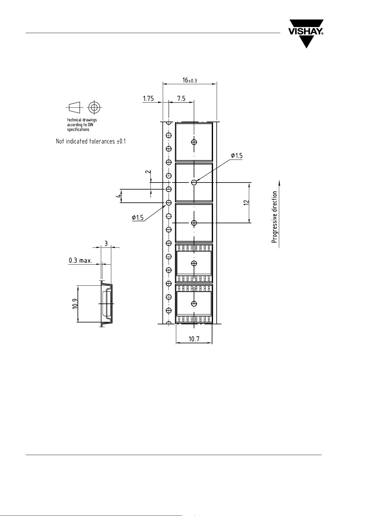
Reel Dimensions
TOIM4232
Vishay Semiconductors
14017
Tape Width A max. N W1 min. W2 max. W3 min. W3 max.
mm mm mm mm mm mm mm
16 330 50 16.4 22.4 15.9 19.4
Document Number 82546
Rev. 1.4, 07-Dec-05
www.vishay.com
11
Page 12
TOIM4232
Vishay Semiconductors
Tape Dimensions in mm
www.vishay.com
12
18241
Document Number 82546
Rev. 1.4, 07-Dec-05
Page 13

TOIM4232
Vishay Semiconductors
Ozone Depleting Substances Policy Statement
It is the policy of Vishay Semiconductor GmbH to
1. Meet all present and future national and international statutory requirements.
2. Regularly and continuously improve the performance of our products, processes, distribution and operating
systems with respect to their impact on the health and safety of our employees and the public, as well as
their impact on the environment.
It is particular concern to control or eliminate releases of those substances into the atmosphere which are
known as ozone depleting substances (ODSs).
The Montreal Protocol (1987) and its London Amendments (1990) intend to severely restrict the use of ODSs
and forbid their use within the next ten years. Various national and international initiatives are pressing for an
earlier ban on these substances.
Vishay Semiconductor GmbH has been able to use its policy of continuous improvements to eliminate the use
of ODSs listed in the following documents.
1. Annex A, B and list of transitional substances of the Montreal Protocol and the London Amendments
respectively
2. Class I and II ozone depleting substances in the Clean Air Act Amendments of 1990 by the Environmental
Protection Agency (EPA) in the USA
3. Council Decision 88/540/EEC and 91/690/EEC Annex A, B and C (transitional substances) respectively.
Vishay Semiconductor GmbH can certify that our semiconductors are not manufactured with ozone depleting
substances and do not contain such substances.
We reserve the right to make changes to improve technical design
and may do so without further notice.
Parameters can vary in different applications. All operating parameters must be validated for each
customer application by the customer. Should the buyer use Vishay Semiconductors products for any
unintended or unauthorized application, the buyer shall indemnify Vishay Semiconductors against all
claims, costs, damages, and expenses, arising out of, directly or indirectly, any claim of personal
damage, injury or death associated with such unintended or unauthorized use.
Vishay Semiconductor GmbH, P.O.B. 3535, D-74025 Heilbronn, Germany
Document Number 82546
Rev. 1.4, 07-Dec-05
www.vishay.com
13
Page 14

Legal Disclaimer Notice
Vishay
Document Number: 91000 www.vishay.com
Revision: 08-Apr-05 1
Notice
Specifications of the products displayed herein are subject to change without notice. Vishay Intertechnology, Inc.,
or anyone on its behalf, assumes no responsibility or liability for any errors or inaccuracies.
Information contained herein is intended to provide a product description only. No license, express or implied, by
estoppel or otherwise, to any intellectual property rights is granted by this document. Except as provided in Vishay's
terms and conditions of sale for such products, Vishay assumes no liability whatsoever, and disclaims any express
or implied warranty, relating to sale and/or use of Vishay products including liability or warranties relating to fitness
for a particular purpose, merchantability, or infringement of any patent, copyright, or other intellectual property right.
The products shown herein are not designed for use in medical, life-saving, or life-sustaining applications.
Customers using or selling these products for use in such applications do so at their own risk and agree to fully
indemnify Vishay for any damages resulting from such improper use or sale.
 Loading...