


TELUX™
Description
The TELUX™ series is a clear, non diffused LED for
applications where supreme luminous flux is required.
It is designed in an industry standard 7.62 mm square
package utilizing highly developed with super bright,
AllnGaP, OMA technology.
The supreme heat dissipation of TELUX™ allows
applications at high ambient temperatures.
All packing units are binned for luminous flux, forward
voltage and color to achieve the most homogenous
light appearance in application.
SAE and ECE color requirements for automobile
application are available for color red.
ESD resistivity 2 kV (HBM) according to MIL STD
883D, method 3015.7.
Features
• Utilizing one of the world’s brightest (AS)
AllnGaP technologies (OMA)
• High luminous flux
• Supreme heat dissipation: R
is 90 K/W
thJP
• High operating temperature:
T
= - 40 to + 110 °C
amb
• Meets SAE and ECE color requirements for
the automobile industry for color red
• Packed in tubes for automatic insertion
• Luminous flux, forward voltage and color
categorized for each tube
• Small mechanical tolerances allow precise usage
of external reflectors or lightguides
• Lead (Pb)-free component
• Component in accordance to RoHS 2002/95/EC
and WEEE 2002/96/EC
e3
TLWR9.2.
Vishay Semiconductors
19232
Applications
Exterior lighting
Tail-, Stop - and Turn Signals of motor vehicles
Replaces small incandescent lamps
Traffic signals and signs
Parts Table
Par t Color, Luminous Intensity Angle of Half Intensity (±ϕ) Technology
TLWR9420 Red, φ
TLWR9421 Red, φ
TLWR9422 Red, φ
TLWR9520 Red, φ
TLWR9521 Red, φ
TLWR9522 Red, φ
Document Number 84792
Rev. 1.3, 17-Oct-05
> 3000 mlm 25 x 68 AllnGaP on GaAs
V
> 3500 mlm 25 x 68 AllnGaP on GaAs
V
> 4000 mlm 25 x 68 AllnGaP on GaAs
V
> 3000 mlm 40 x 90 AllnGaP on GaAs
V
> 3500 mlm 40 x 90 AllnGaP on GaAs
V
> 4000 mlm 40 x 90 AllnGaP on GaAs
V
www.vishay.com
1

TLWR9.2.
Vishay Semiconductors
Absolute Maximum Ratings
T
= 25 °C, unless otherwise specified
amb
TLWR9.2.
Parameter Test condition Symbol Val ue Unit
Reverse voltage I
DC Forward current T
Surge forward current t
Junction temperature T
Operating temperature range T
Storage temperature range T
Soldering temperature t ≤ 5 s, 1.5 mm from body
Thermal resistance junction/
ambient
Optical and Electrical Characteristics
T
= 25 °C, unless otherwise specified
amb
Red
TLWR9.2.
Parameter Test condition Part Symbol Min Ty p. Max Unit
Total flux I
Dominant wavelength I
Peak wavelength I
Angle of half intensity I
Forward voltage I
Reverse voltage V
Temperature coefficient < λ
Temperature coefficient V
F
= 100 μAV
R
≤ 85 °C I
amb
≤ 10 μsI
p
preheat temperature
F
FSM
amb
stg
T
sd
R
j
100 °C/ 30 sec.
with cathode heatsink
of 70 mm
F
2
= 70 mA, R
= 200 °K/W TLWR9420 φ
thJA
R
thJA
TLWR9421 φ
TLWR9422 φ
TLWR9520 φ
TLWR9521 φ
TLWR9522 φ
= 70 mA, R
F
= 70 mA, R
F
= 70 mA, R
F
= 200 °K/W λ
thJA
= 200 °K/W λ
thJA
= 200 °K/W TLWR942x ϕ 25 x 68 deg
thJA
TLWR952x ϕ 40 x 90 deg
= 70 mA, R
F
IF = 70 mA TCλ
d
= 200 °K/W V
thJA
IF = 70 mA, T > - 25 °C TC
10 V
70 mA
0.1 A
125 °C
- 40 to + 110 °C
- 55 to + 110 °C
260 °C
200 K/W
3000 3700 mlm
V
3500 4200 mlm
V
4000 5000 mlm
V
3000 3700 mlm
V
3500 4200 mlm
V
4000 5000 mlm
V
d
p
R
611 615 634 nm
624 nm
1.83 2.5 3.03 V
F
10 20 V
d
VF
0.05 nm/K
- 2.0 mV/K
Forward Voltage Classification
Group Forward Voltage (V)
Y 1.83 2.07
Z 1.95 2.19
0 2.07 2.31
1 2.19 2.43
2 2.31 2.55
3 2.43 2.67
4 2.55 2.79
5 2.67 2.91
6 2.79 3.03
www.vishay.com
2
min max
Document Number 84792
Rev. 1.3, 17-Oct-05

Vishay Semiconductors
Color Classification
Group Dominant Wavelength (nm)
min max
1 611 618
2 614 622
3 616 634
Luminous Flux Classification
Group Luminous Intensity (mlm)
min max
F 3000 4200
G 3500 4800
H 4000 6100
I 5000 7300
K 6000 9700
Typical Characteristics (Tamb = 25 °C unless otherwise specified)
TLWR9.2.
100
Red
R
=200K/W
thJA
0
0 20406080 100 120
T
– Ambient Temperature ( C )
amb
15983
80
60
40
20
F
I – Forward Current ( mA )
Figure 1. Forward Current vs. Ambient Temperature
0.12
0.10
0.08
0.06
0.04
F
I –Forward Current (A)
0.02
0.005
0.05
0.5
1.0
TLWR952x
0.8
ntensity
0.6
us I
0.4
0.2
Relative Lumino
0
-90° -60° -30° 30° 60° 90°0°
19732
Off Axis Angle
horizontal
vertical
Figure 3. Rel. Luminous Intensity vs. Off Axis
ntensity
us I
Relative Lumino
1.0
0.8
0.6
0.4
0.2
TLWR942x
horizontal
vertical
0.00
10–510–410–310–210–1100 10110
16731
tp – Pulse Length (ms)
Figure 2. Forward Current vs. Pulse Length
Document Number 84792
Rev. 1.3, 17-Oct-05
2
0
-90° -60° -30° 0° 30° 60° 90°
19733
Off Axis Angle
Figure 4. Rel. Luminous Intensity vs. Off Axis
www.vishay.com
3

TLWR9.2.
Vishay Semiconductors
10
Red
1
0.1
Vrel
I - Relative Luminous Intensity
0.01
1 10 100
15978
IF- Forward Current ( mA )
230
220
210
200
190
thJA
R in K/W
180
170
160
0 50 100 150 200 250 300
16009
Cathode Padsize in mm
Padsize 8 mm
per Anode Pin
2
2
Figure 5. Relative Luminous Flux vs. Forward Current
1.8
1.6
Red
IF=70mA
1.4
1.2
1.0
0.8
0.6
– Relative Luminous Flux
0.4
V rel
Φ
0.2
0.0
-40 -20 0 2 0 40 60 80 100
T
18021
– Ambient Temperature ( °C)
amb
Figure 6. Rel. Luminous Flux vs. Ambient Temperature
Vrel
I - Relative Luminous Intensity
16007
1.2
1.1
1.0
0.9
0.8
0.7
0.6
0.5
0.4
0.3
0.2
0.1
0.0
Red
570 580 590 600 610 620 630 640 650 660 670
λ - Wavelength ( nm )
Figure 8. Thermal Resistance Junction Ambient vs. Cathode
Padsize
Figure 7. Relative Intensity vs. Wavelength
www.vishay.com
4
Document Number 84792
Rev. 1.3, 17-Oct-05

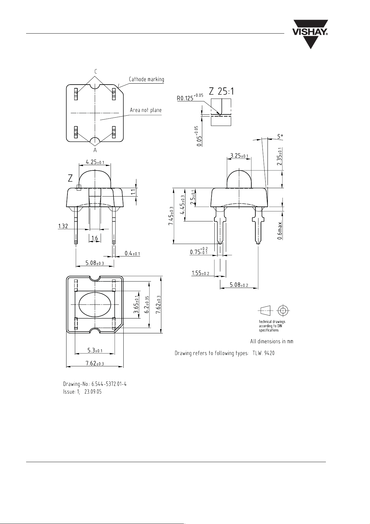
Package Dimensions in mm
TLWR9.2.
Vishay Semiconductors
Document Number 84792
Rev. 1.3, 17-Oct-05
19734
www.vishay.com
5
TLWR9.2.
Vishay Semiconductors
Package Dimensions in mm
www.vishay.com
6
19735
Document Number 84792
Rev. 1.3, 17-Oct-05

Packing Information
7
Fan Fold Box
TLWR9.2.
Vishay Semiconductors
Label of Fan Fold Box
A
B C D E F
106
16491
A) Type of component
B) Manufacturing plant
C) SEL – Selection Code (Bin)
Digit 1 – code for Luminous Flux group
H
Digit 2 – code for Dominant Wavelengthgroup
Digit 3 – code for Forward Voltage group
3
D) Date Code year/week
E) Day Code (e. g. 5: Friday)
F) Batch No.
G) Total quantity
H) Company code
G
18999
Note: Any distance between bar code and character
is more than 1mm.
Document Number 84792
Rev. 1.3, 17-Oct-05
www.vishay.com
7

TLWR9.2.
Vishay Semiconductors
Example for TELUX tube label
90
52
A
B
C D E F G H
A) Bar code
B) Type of component
C) Manufacturing plant
D) SEL – Selection code (Bin)
Digit1 – code for Luminous Flux group
Digit2 – code for Dominant Wavelength group
Digit3 – code for Forward Voltage group
E) Date code
Tube with Bar code label
8
16490
F) Batch No.
G) Total quantity
H) Company code
www.vishay.com
8
18989
Figure 9. Drawing proportions not scaled
Document Number 84792
Rev. 1.3, 17-Oct-05

TLWR9.2.
Vishay Semiconductors
Ozone Depleting Substances Policy Statement
It is the policy of Vishay Semiconductor GmbH to
1. Meet all present and future national and international statutory requirements.
2. Regularly and continuously improve the performance of our products, processes, distribution and operating
systems with respect to their impact on the health and safety of our employees and the public, as well as
their impact on the environment.
It is particular concern to control or eliminate releases of those substances into the atmosphere which are
known as ozone depleting substances (ODSs).
The Montreal Protocol (1987) and its London Amendments (1990) intend to severely restrict the use of ODSs
and forbid their use within the next ten years. Various national and international initiatives are pressing for an
earlier ban on these substances.
Vishay Semiconductor GmbH has been able to use its policy of continuous improvements to eliminate the use
of ODSs listed in the following documents.
1. Annex A, B and list of transitional substances of the Montreal Protocol and the London Amendments
respectively
2. Class I and II ozone depleting substances in the Clean Air Act Amendments of 1990 by the Environmental
Protection Agency (EPA) in the USA
3. Council Decision 88/540/EEC and 91/690/EEC Annex A, B and C (transitional substances) respectively.
Vishay Semiconductor GmbH can certify that our semiconductors are not manufactured with ozone depleting
substances and do not contain such substances.
We reserve the right to make changes to improve technical design
and may do so without further notice.
Parameters can vary in different applications. All operating parameters must be validated for each
customer application by the customer. Should the buyer use Vishay Semiconductors products for any
unintended or unauthorized application, the buyer shall indemnify Vishay Semiconductors against all
claims, costs, damages, and expenses, arising out of, directly or indirectly, any claim of personal
damage, injury or death associated with such unintended or unauthorized use.
Vishay Semiconductor GmbH, P.O.B. 3535, D-74025 Heilbronn, Germany
Document Number 84792
Rev. 1.3, 17-Oct-05
www.vishay.com
9

Legal Disclaimer Notice
Vishay
Document Number: 91000 www.vishay.com
Revision: 08-Apr-05 1
Notice
Specifications of the products displayed herein are subject to change without notice. Vishay Intertechnology, Inc.,
or anyone on its behalf, assumes no responsibility or liability for any errors or inaccuracies.
Information contained herein is intended to provide a product description only. No license, express or implied, by
estoppel or otherwise, to any intellectual property rights is granted by this document. Except as provided in Vishay's
terms and conditions of sale for such products, Vishay assumes no liability whatsoever, and disclaims any express
or implied warranty, relating to sale and/or use of Vishay products including liability or warranties relating to fitness
for a particular purpose, merchantability, or infringement of any patent, copyright, or other intellectual property right.
The products shown herein are not designed for use in medical, life-saving, or life-sustaining applications.
Customers using or selling these products for use in such applications do so at their own risk and agree to fully
indemnify Vishay for any damages resulting from such improper use or sale.
 Loading...