

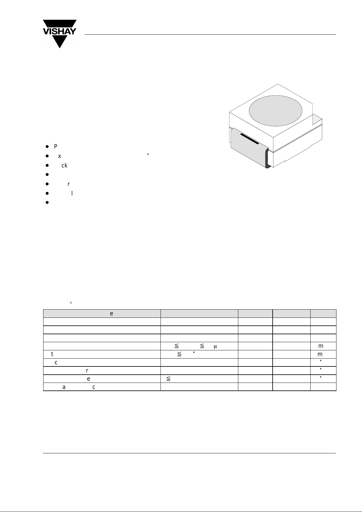
Silicon NPN Phototransistor
Description
TEMT3700 is a high speed silicon NPN epitaxial
planar phototransistor in a miniature PL–CC–2 package for surface mounting on printed boards. Due to its
waterclear epoxy lens the device is sensitive to visible
and near infrared radiation.
Features
D
PL–CC–2 SMD package
D
Extra wide viewing angle ϕ = ± 60
D
Package notch = collector
D
Base terminal not connected
D
Fast response times
D
Suitable for visible and near infrared radiation
D
Matches with IR emitter TSMS3700
°
TEMT3700
Vishay Semiconductors
94 8553
Applications
Miniature switches
Counters and sorters
Interrupters
Tape and card readers
Encoders
Position sensors
Absolute Maximum Ratings
T
= 25_C
amb
Parameter Test Conditions Symbol Value Unit
Collector Emitter Voltage V
Emitter Collector Voltage V
Collector Current I
Peak Collector Current tp/T x 0.1, tp x 10ms I
Total Power Dissipation T
Junction Temperature T
Storage Temperature Range T
Soldering Temperature t x 3 s T
Thermal Resistance Junction/Ambient R
x 55 °C P
amb
CEO
ECO
C
CM
tot
j
stg
sd
thJA
70 V
5 V
50 mA
100 mA
100 mW
100
–55...+100
260
450 K/W
°
C
°
C
°
C
Document Number 81555
Rev. 3, 10-Apr-01
www.vishay.com
1 (6)
TEMT3700
Vishay Semiconductors
Basic Characteristics
T
= 25_C
amb
Parameter Test Conditions Symbol Min Typ Max Unit
Collector Emitter Breakdown
Voltage
Collector Dark Current VCE = 20 V, E = 0 I
Collector Emitter Capacitance VCE = 5 V, f = 1 MHz, E=0 C
Collector Light Current Ee = 1 mW/cm2,
Angle of Half Sensitivity ϕ ±60 deg
Wavelength of Peak Sensitivity
Range of Spectral Bandwidth
Collector Emitter Saturation
Voltage
Rise Time / Fall Time VS = 5 V, IC = 1 mA,
Cut–Off Frequency VS = 5 V, IC = 2 mA,
IC = 1 mA V
l
= 950 nm, VCE = 5 V
Ee = 1 mW/cm2,
l
= 950 nm, IC = 0.1 mA
l
= 950 nm, RL = 1 k
W
VS = 5 V, IC = 1 mA,
l
= 950 nm, R
R
= 100
L
W
= 100
L
W
(BR)CE
O
CEO
CEO
I
ca
l
p
l
0.5
V
CEsat
tr / t
tr / t
f
c
70 V
1 200 nA
3 pF
0.25 0.5 mA
830 nm
620...980 nm
0.15 0.3 V
f
f
6
2
180 kHz
m
s
m
s
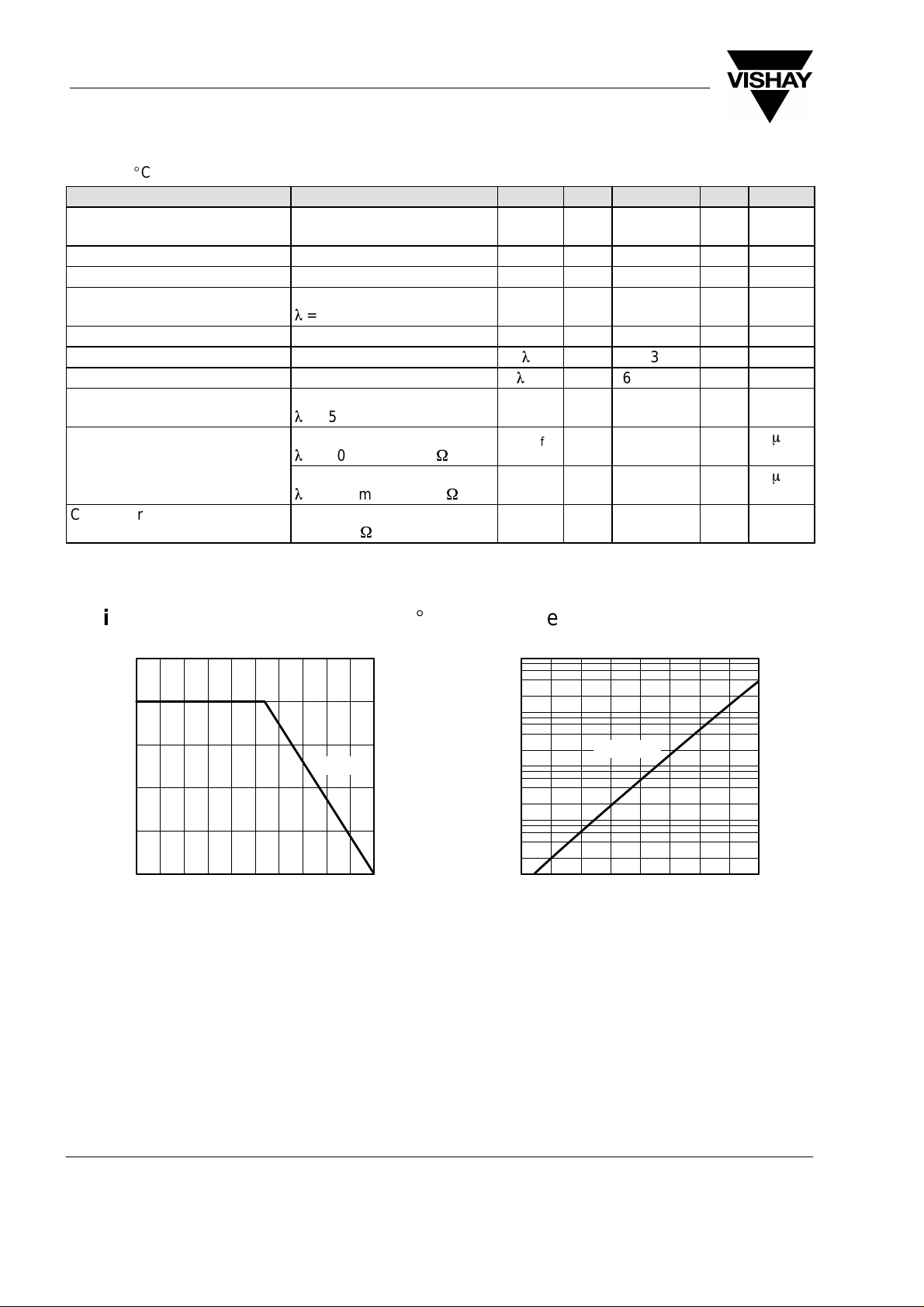
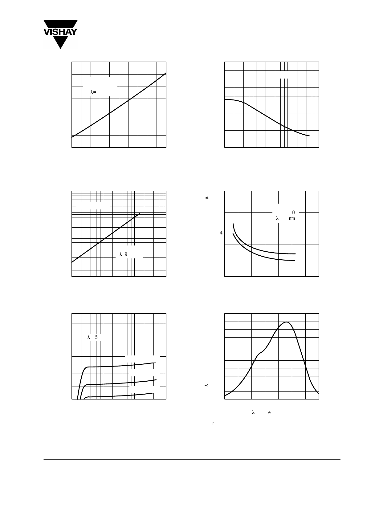
Typical Characteristics (T
125
100
75
50
25
tot
P – Total Power Dissipation ( mW )
0
020406080
T
94 8308
Figure 1. Total Power Dissipation vs.
– Ambient Temperature ( °C )
amb
Ambient Temperature
= 25_C unless otherwise specified)
amb
4
10
3
10
VCE=20V
40 60 80
T
– Ambient Temperature ( °C )
amb
CEO
I – Collector Dark Current ( nA )
94 8304
2
10
1
10
0
10
20
R
thJA
100
Figure 2. Collector Dark Current vs. Ambient Temperature
100
www.vishay.com
2 (6) Rev. 3, 10-Apr-01
Document Number 81555
TEMT3700
Vishay Semiconductors
2.0
1.8
1.6
VCE=5V
E
=1mW/cm
e
l
=950nm
2
1.4
1.2
1.0
ca rel
0.8
I – Relative Collector Current
0.6
0
20 40 60 80
94 8239
T
– Ambient Temperature ( °C )
amb
Figure 3. Relative Collector Current vs.
Ambient Temperature
10
TEMT 3704
1
0.1
100
10
8
f=1MHz
6
4
2
CEO
C – Collector Emitter Capacitance ( pF )
0
0.1 1 10
94 8294
– Collector Emitter Voltage ( V )
V
CE
Figure 6. Collector Emitter Capacitance vs.
Collector Emitter Voltage
8
m
6
4
VCE=5V
R
=100
L
l
=950nm
W
100
0.01
ca
I – Collector Light Current ( mA )
l
=950nm
0.001
0.01 0.1 1
VCE=5V
94 8316
Ee – Irradiance ( mW/cm2 )
Figure 4. Collector Light Current vs. Irradiance
10
l
=950nm
1
Ee=1mW/cm
0.5mW/cm
ca
I – Collector Light Current ( mA )
0.2mW/cm
0.1
0.1 1 10
94 8317
VCE – Collector Emitter Voltage ( V )
Figure 5. Collector Light Current vs.
Collector Emitter Voltage
t
2
off
on
t / t – Turn on / Turn off Time ( s )
94 8293
0
024 6 12
IC – Collector Current ( mA )
10
off
t
on
108
14
Figure 7. Turn On/Turn Off Time vs. Collector Current
1.0
0.8
0.6
2
2
2
0.4
rel
0.2
l
S ( ) – Relative Spectral Sensitivity
0
100
400 600 1000
l
– Wavelength ( nm )94 8348
800
Figure 8. Relative Spectral Sensitivity vs. Wavelength
Document Number 81555
Rev. 3, 10-Apr-01
www.vishay.com
3 (6)

TEMT3700
Vishay Semiconductors
0°
10°20
°
30°
1.0
0.9
0.8
rel
S – Relative Sensitivity
0.7
0.4 0.2 0 0.2 0.4
0.6
94 8318
Figure 9. Relative Radiant Sensitivity vs.
Angular Displacement
Dimensions in mm
40°
50°
60°
70°
80°
0.6
95 11316
www.vishay.com
4 (6) Rev. 3, 10-Apr-01
Document Number 81555
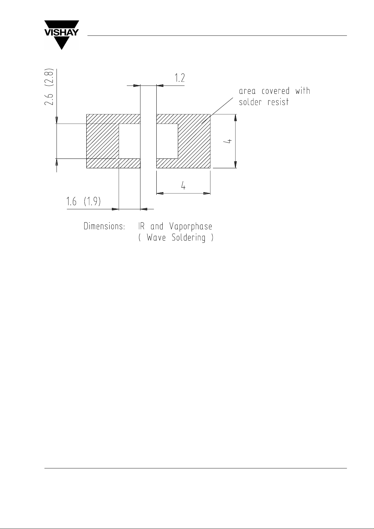
Solderpad Design in mm
TEMT3700
Vishay Semiconductors
95 10966
Document Number 81555
Rev. 3, 10-Apr-01
www.vishay.com
5 (6)

TEMT3700
Vishay Semiconductors
Ozone Depleting Substances Policy Statement
It is the policy of Vishay Semiconductor GmbH to
1. Meet all present and future national and international statutory requirements.
2. Regularly and continuously improve the performance of our products, processes, distribution and operating
systems with respect to their impact on the health and safety of our employees and the public, as well as their
impact on the environment.
It is particular concern to control or eliminate releases of those substances into the atmosphere which are known as
ozone depleting substances (ODSs).
The Montreal Protocol (1987) and its London Amendments (1990) intend to severely restrict the use of ODSs and
forbid their use within the next ten years. V arious national and international initiatives are pressing for an earlier ban
on these substances.
Vishay Semiconductor GmbH has been able to use its policy of continuous improvements to eliminate the use of
ODSs listed in the following documents.
1. Annex A, B and list of transitional substances of the Montreal Protocol and the London Amendments respectively
2. Class I and II ozone depleting substances in the Clean Air Act Amendments of 1990 by the Environmental
Protection Agency (EPA) in the USA
3. Council Decision 88/540/EEC and 91/690/EEC Annex A, B and C (transitional substances) respectively.
Vishay Semiconductor GmbH can certify that our semiconductors are not manufactured with ozone depleting
substances and do not contain such substances.
We reserve the right to make changes to improve technical design and may do so without further notice.
Parameters can vary in different applications. All operating parameters must be validated for each customer application
by the customer. Should the buyer use Vishay Semiconductors products for any unintended or unauthorized application, the
buyer shall indemnify Vishay Semiconductors against all claims, costs, damages, and expenses, arising out of, directly or
indirectly , any claim of personal damage, injury or death associated with such unintended or unauthorized use.
Vishay Semiconductor GmbH, P.O.B. 3535, D-74025 Heilbronn, Germany
Telephone: 49 (0)7131 67 2831, Fax number: 49 (0)7131 67 2423
www.vishay.com
6 (6) Rev. 3, 10-Apr-01
Document Number 81555

This datasheet has been download from:
www.datasheetcatalog.com
Datasheets for electronics components.
 Loading...