

Page 1
VISHAY
17294
C
CE
AC
1
2
3
4
V
D E
TCLD1000
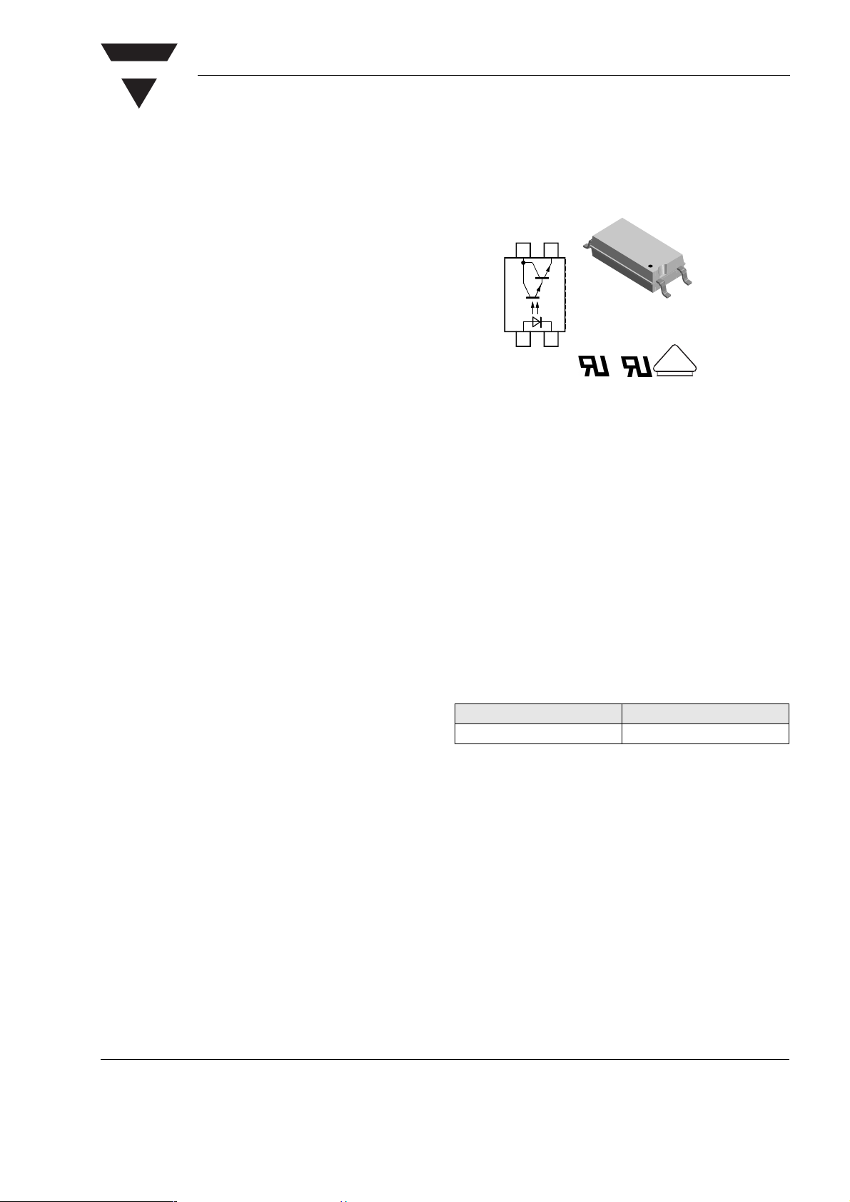
Vishay Semiconductors
Optocoupler, Photodarlington Output, SOP-4L, Long Mini-Flat
Package
Features
• Low profile package
• Darlington output
• Extra low coupling capacity - typical 0.2 pF
• High Common Mode Rejection
• Creepage current resistance according to VDE
0303/IEC 60112 Comparative Tracking Index:
CTI ≥ 175
• Thickness through insulation ≥ 0.75 mm
• Creepage distance > 8 mm
• Tested acc. 60950: AM4: 1997 clause 2.9.6.
Agency Approvals
• UL - File No. E76222 System Code W
• UL 1577
• CSA 22.2 bulletin 5A, Double Protection
• BSI IEC60950 IEC60965
• DIN EN 60747-5-2(VDE0884)
DIN EN 60747-5-5 pending
Applications
Switch-mode power supplies
Line receiver
Computer peripheral interface
Microprocessor system interface
Reinforced Isolation provides circuit protection
against electrical shock (Safety Class II)
Circuits for safe protective separation against electri-
cal shock according to safety class II (reinforced isolation):
• For appl. class I - IV at mains voltage ≤ 300 V
• For appl. class I - III at mains voltage ≤ 600 V according to DIN EN 60747-5-2(VDE0884)/ DIN EN 607475-5 pending, table 2.
Description
The TCLD1000 consists of a darlington phototransistor optically coupled to a gallium arsenide infraredemitting diode in a 4-lead SO6L package.
The elements are mounted on one leadframe, provide
a fixed distance between input and output for highest
safety requirements.
Order Information
Part Remarks
TCLD1000 CTR > 600 %, SMD-4
Document Number 83516
Rev. 1.6, 20-Apr-04
www.vishay.com
1
Page 2
TCLD1000
VISHAY
Vishay Semiconductors
Absolute Maximum Ratings
T
= 25 °C, unless otherwise specified
amb
Stresses in excess of the absolute Maximum Ratings can cause permanent damage to the device. Functional operation of the device is
not implied at these or any other conditions in excess of those given in the operational sections of this document. Exposure to absolute
Maximum Rating for extended periods of the time can adversely affect reliability.
Input
Parameter Test condition Symbol Val ue Unit
Reverse voltage V
Forward current I
Forward surge current t
Power dissipation P
Junction temperature T
≤ 10 µsI
p
R
F
FSM
diss
j
6V
60 mA
1.5 A
100 mW
125 °C
Output
Parameter Test condition Symbol Val ue Unit
Collector emitter voltage V
Emitter collector voltage V
Collector current I
Collector peak current t
Power dissipation P
Junction temperature T
/T = 0.5, tp ≤ 10 ms I
p
CEO
ECO
C
CM
diss
j
35 V
7V
80 mA
100 mA
150 mW
125 °C
Coupler
Parameter Test condition Symbol Val ue Unit
Isolation test voltage (RMS) V
Total power dissipation P
Operating ambient temperature
range
Storage temperature range T
Soldering temperature T
T
ISO
tot
amb
stg
sld
5000 V
250 mW
- 40 to + 100 °C
- 40 to + 100 °C
240 °C
RMS
Electrical Characteristics
T
= 25 °C, unless otherwise specified
amb
Minimum and maximum values are testing requirements. Typical values are characteristics of the device and are the result of engineering
evaluation. Typical values are for information only and are not part of the testing requirements.
Input
Parameter Test condition Symbol Min Ty p. Max Unit
Forward voltage I
Junction capacitance V
= ± 50 mA V
F
= 0 V, f = 1 MHz C
R
F
j
1.25 1.6 V
50 pF
Output
Parameter Test condition Symbol Min Ty p. Max Unit
Collector emitter voltage I
Emitter collector voltage I
Collector-emitter cut-off current V
= 1 mA V
C
= 100 µAV
E
= 20 V, If = 0, E = 0 I
CE
CEO
ECO
CEO
35 V
7V
100 nA
www.vishay.com
2
Document Number 83516
Rev. 1.6, 20-Apr-04
Page 3
VISHAY
Coupler
Parameter Test condition Symbol Min Ty p. Max Unit
Collector emitter saturation
voltage
Cut-off frequency V
Coupling capacitance f = 1 MHz C
Current Transfer Ratio
Parameter Test condition Symbol Min Ty p. Max Unit
I
C/IF
Maximum Safety Ratings
(according to DIN EN 60747-5-2(VDE0884)/ DIN EN 60747-5-5 pending) see figure 1
This optocoupler is suitable for safe electrical isolation only within the safety ratings.
Compliance with the safety ratings shall be ensured by means of suitable protective circuits.
= 10 mA, IC = 1 mA V
I
F
= 5 V, IF = 10 mA,
CE
R
= 100 Ω
L
VCE = 2 V, IF = 1 mA CTR 600 800 %
CEsat
f
c
k
TCLD1000
Vishay Semiconductors
0.3 V
10 kHz
0.3 pF
Input
Parameter Test condition Symbol Min Ty p. Max Unit
Forward current I
Output
Parameter Test condition Symbol Min Ty p. Max Unit
Power dissipation T
≤ 25 °C P
amb
Coupler
Parameter Test condition Symbol Min Ty p. Max Unit
Rated impulse voltage V
Safety temperature T
Insulation Rated Parameters
Parameter Test condition Symbol Min Ty p. Max Unit
Partial discharge test voltage Routine test
Partial discharge test voltage Lot test (sample test)
Insulation resistance V
100 %, t
t
= 60 s, t
Tr
(see figure 2)
IO
V
IO
V
IO
(constru ction test on ly)
= 1 s V
test
= 10 s,
test
= 500 V R
= 500 V, T
= 500 V, T
= 100 °C R
amb
= 150 °C
amb
V
F
diss
IOTM
si
pd
IOTM
V
pd
IO
IO
R
IO
130 mA
265 mW
8kV
150 °C
1.6 kV
8kV
1.3 kV
10
10
10
12
11
9
Ω
Ω
Ω
Document Number 83516
Rev. 1.6, 20-Apr-04
www.vishay.com
3
Page 4

TCLD1000
Vishay Semiconductors
300
250
200
150
100
Phototransistor
Psi ( mW )
V
V
V
IOTM
V
IOWM
IORM
VISHAY
t1, t2 = 1 to 10 s
, t4 = 1 s
t
3
t
= 10 s
test
t
= 12 s
stres
Pd
50
tot
P – Total Power Dissipation ( mW )
0
0 25 50 75 125
94 9182
Fig. 1 Derating diagram
IR-Diode
Isi ( mA )
100
Tsi – Safety Temperature ( °C )
150
13930
0
t
1
tTr = 60 s
t
2
t
t3t
t
stres
Fig. 2 Test pulse diagram for sample test according to DIN EN
60747-5-2(VDE0884)/ DIN EN 60747-; IEC60747
Switching Characteristics
Parameter Test condition Symbol Min Ty p . Max Unit
Rise time V
= 2 V, IC = 10 mA, RL = 100 Ω (see
CE
figure 1)
Turn-off time V
= 2 V, IC = 10 mA, RL = 100 Ω (see
CE
figure 1)
+V
0
R
G
t
p
T
= 50 Ω
= 0.01
I
I
F
F
CC
IC = 10 mA;
tp = 50 ms
Channel I
Channel II
14779
50 Ω
R
L
Fig. 3 Test circuit, non-saturated operation
Oscilloscope
= 1 MΩ
R
I
C
= 20 pF
I
t
r
t
off
I
F
0
I
C
100%
90%
10%
0
t
p
t
d
t
r
t
(= td+tr) turn-on time
on
t
r
t
d
t
on
pulse duration
delay time
rise time
Fig. 4 Switching Times
300 µs
250 µs
t
p
t
t
f
s
t
off
t
s
t
f
t
(= ts+tf) turn-off time
off
96 11698
storage time
fall time
test
4
t
t
t
www.vishay.com
4
Document Number 83516
Rev. 1.6, 20-Apr-04
Page 5

VISHAY
TCLD1000
Vishay Semiconductors
Typical Characteristics (T
1.3
IF=10mA
1.2
1.1
1.0
F
0.9
V – Forward Voltage ( V )
0.8
0 20406080100
T
14389
– Ambient Temperature (°C )
amb
= 25 °C unless otherwise specified)
amb
Fig. 5 Forward Voltage vs. Ambient Temperature
1000.0
100.0
100000
VCE=10V
I
=0
10000
1000
with open Base ( nA)
CEO
I – Collector Dark Current,
14392
F
100
10
1
20 30 40 50 60 70 80 90 100
T
– Ambient Temperature (°C )
amb
Fig. 8 Collector Dark Current vs. Ambient Temperature
1000.0
VCE=2V
100.0
10.0
1.0
F
I – Forward Current ( mA )
0.1
0.0 0.2 0.4 0.6 0.8 1.0 1.2 1.4 1.6 1.8 2.0
14390
VF– Forward Voltage(V)
Fig. 6 Forward Current vs. Forward Voltage
1.5
VCE=5V
1.4
I
=1mA
F
1.3
1.2
1.1
1.0
0.9
0.8
0.7
0.6
rel
0.5
CTR – Relative Current Transfer Ratio
–30–20–100 102030405060708090100
T
14391
– Ambient Temperature (°C )
amb
10.0
1.0
C
I – Collector Current ( mA)
0.1
0.1 1.0 10.0 100.0
14393
IF– Forward Current ( mA )
Fig. 9 Collector Current vs. Forward Current
100.0
10.0
1.0
C
I – Collector Current ( mA)
0.1
0.1 1.0 10.0 100.0
14394
VCE– Collector Emitter Voltage(V)
IF=2mA
1mA
0.5mA
0.2mA
0.1mA
Fig. 7 Relative Current Transfer Ratio vs. Ambient Temperature
Document Number 83516
Rev. 1.6, 20-Apr-04
Fig. 10 Collector Current vs. Collector Emitter Voltage
www.vishay.com
5
Page 6

TCLD1000
Vishay Semiconductors
Package Dimensions in mm
VISHAY
15243
www.vishay.com
6
Document Number 83516
Rev. 1.6, 20-Apr-04
Page 7

VISHAY
TCLD1000
Vishay Semiconductors
Ozone Depleting Substances Policy Statement
It is the policy of Vishay Semiconductor GmbH to
1. Meet all present and future national and international statutory requirements.
2. Regularly and continuously improve the performance of our products, processes, distribution and
operatingsystems with respect to their impact on the health and safety of our employees and the public, as
well as their impact on the environment.
It is particular concern to control or eliminate releases of those substances into the atmosphere which are
known as ozone depleting substances (ODSs).
The Montreal Protocol (1987) and its London Amendments (1990) intend to severely restrict the use of ODSs
and forbid their use within the next ten years. Various national and international initiatives are pressing for an
earlier ban on these substances.
Vishay Semiconductor GmbH has been able to use its policy of continuous improvements to eliminate the
use of ODSs listed in the following documents.
1. Annex A, B and list of transitional substances of the Montreal Protocol and the London Amendments
respectively
2. Class I and II ozone depleting substances in the Clean Air Act Amendments of 1990 by the Environmental
Protection Agency (EPA) in the USA
3. Council Decision 88/540/EEC and 91/690/EEC Annex A, B and C (transitional substances) respectively.
Vishay Semiconductor GmbH can certify that our semiconductors are not manufactured with ozone depleting
substances and do not contain such substances.
We reserve the right to make changes to improve technical design
and may do so without further notice.
Parameters can vary in different applications. All operating parameters must be validated for each
customer application by the customer. Should the buyer use Vishay Semiconductors products for any
unintended or unauthorized application, the buyer shall indemnify Vishay Semiconductors against all
claims, costs, damages, and expenses, arising out of, directly or indirectly, any claim of personal
damage, injury or death associated with such unintended or unauthorized use.
Vishay Semiconductor GmbH, P.O.B. 3535, D-74025 Heilbronn, Germany
Telephone: 49 (0)7131 67 2831, Fax number: 49 (0)7131 67 2423
Document Number 83516
Rev. 1.6, 20-Apr-04
www.vishay.com
7
 Loading...