

TCDT1100(G) Series
Vishay Telefunken
Optocoupler with Phototransistor Output
Description
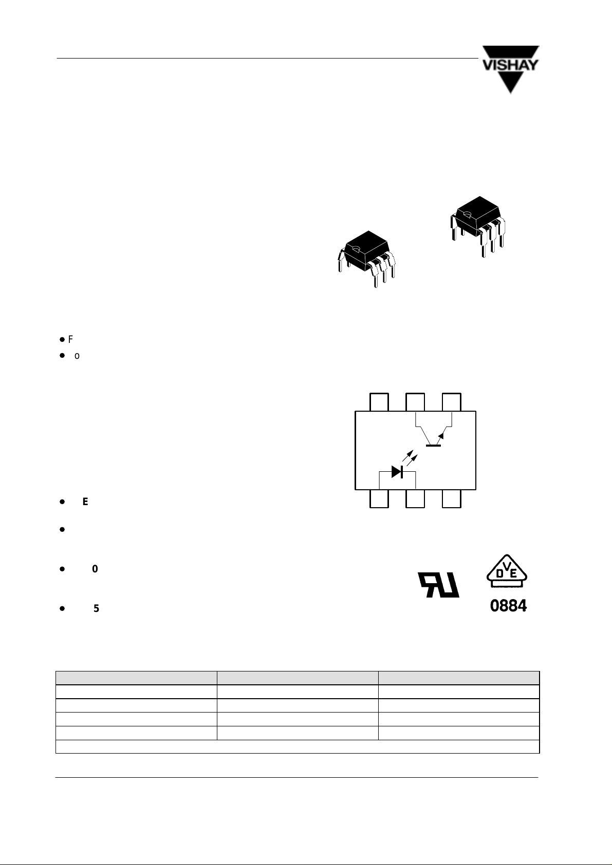
The TCDT1100(G) series consists of a phototransistor optically coupled to a gallium arsenide
infrared-emitting diode in a 6-lead plastic dual inline
package.
The elements are mounted on one leadframe using
a coplanar technique, providing a fixed distance
between input and output for highest safety
requirements.
Applications
Circuits for safe protective separation against
electrical shock according to safety class II
(reinforced isolation):
D
For appl. class I – IV at mains voltage ≤ 300 V
D
For appl. class I – III at mains voltage ≤ 600 V
according to VDE 0884, table 2, suitable for:
Switch-mode power supplies, line receiver,
computer peripheral interface, microprocessor
system interface.
VDE Standards
These couplers perform safety functions according
to the following equipment standards:
D
VDE 0884
Optocoupler for electrical safety requirements
D
IEC 950/EN 60950
Office machines (applied for reinforced isolation
for mains voltage ≤ 400 V
D
VDE 0804
Telecommunication apparatus and data
processing
D
IEC 65 Safety for mains-operated electronic and
related household apparatus
RMS
)
14827
nc
C
65
1
2
A (+) C (–) nc
E
4
94 9222
3
Order Instruction
Ordering Code CTR Ranking Remarks
TCDT1100/ TCDT1100G
TCDT1101/ TCDT1101G
TCDT1102/ TCDT1102G
TCDT1103/ TCDT1103G
1)
G = Leadform 10.16 mm; G is not market on the body
1)
1)
1)
1)
> 40%
40 to 80%
63 to 125%
100 to 200%
Rev. A3, 11–Jan–99208
Features
TCDT1100(G) Series
Vishay Telefunken
Approvals:
D
BSI: BS EN 41003, BS EN 60095 (BS 415),
BS EN 60950 (BS 7002),
Certificate number 7081 and 7402
D
FIMKO (SETI): EN 60950,
D
Creepage current resistance according to
VDE 0303/IEC 1 12
Comparative Tracking Index: CTI = 275
D
Thickness through insulation ≥ 0.75 mm
Certificate number 12399
D
Underwriters Laboratory (UL) 1577 recognized,
file number E-76222
D
VDE 0884, Certificate number 94778
VDE 0884 related features:
D
Rated impulse voltage (transient overvoltage)
= 6 kV peak
V
IOTM
D
Isolation test voltage (partial discharge test
voltage) V
D
Rated isolation voltage (RMS includes DC)
V
IOWM
D
Rated recurring peak voltage (repetitive)
V
IORM
= 1.6 kV
pd
= 600 V
= 600 V
(848 V peak)
RMS
RMS
General features:
D
Isolation materials according to UL94-VO
D
Pollution degree 2
(DIN/VDE 0110/ resp. IEC 664)
D
Climatic classification 55/100/21 (IEC 68 part 1)
D
Special construction:
Therefore, extra low coupling capacity of
typical 0.2 pF, high Common Mode Rejection
D
Low temperature coefficient of CTR
D
CTR offered in 4 groups
D
Base not connected
D
Coupling System A
Absolute Maximum Ratings
Input (Emitter)
Parameter Test Conditions Symbol Value Unit
Reverse voltage V
Forward current I
Forward surge current tp ≤ 10 ms I
Power dissipation T
Junction temperature T
≤ 25°C P
amb
R
F
FSM
V
5 V
60 mA
3 A
100 mW
j
125
°
C
Output (Detector)
Parameter Test Conditions Symbol Value Unit
Collector emitter voltage V
Emitter collector voltage V
Collector current I
Collector peak current tp/T = 0.5, tp ≤ 10 ms I
Power dissipation T
≤ 25°C P
amb
Junction temperature T
CEO
ECO
C
CM
V
j
32 V
7 V
50 mA
100 mA
150 mW
125
°
C
Coupler
Parameter Test Conditions Symbol V alue Unit
AC Isolation test voltage (RMS) t = 1 min V
Total power dissipation T
≤ 25°C P
amb
Ambient temperature range T
Storage temperature range T
Soldering temperature 2 mm from case t ≤ 10 s T
IO
tot
amb
stg
sd
Rev. A3, 11–Jan–99 209
3.75 kV
250 mW
–55 to +100
–55 to +125
260
°
C
°
C
°
C
TCDT1100(G) Series
C F
CE F
Vishay Telefunken
Electrical Characteristics (T
amb
= 25°C)
Input (Emitter)
Parameter Test Conditions Symbol Min. Typ. Max. Unit
Forward voltage IF = 50 mA V
Junction capacitance VR = 0, f = 1 MHz C
Output (Detector)
Parameter Test Conditions Symbol Min. Typ. Max. Unit
Collector emitter voltage IC = 1 mA V
Emitter collector voltage IE = 100 mA V
Collector emitter cut-off
current
VCE = 20 V, If = 0, E = 0 I
Coupler
Parameter Test Conditions Symbol Min. Typ. Max. Unit
Collector emitter
saturation voltage
Cut-off frequency VCE = 5 V, IF = 10 mA,
Coupling capacitance f = 1 MHz C
IF = 10 mA, IC = 1 mA V
R
L
= 100
W
F
j
CEO
ECO
CEO
CEsat
f
c
k
1.25 1.6 V
50 pF
32 V
7 V
200 nA
0.3 V
110 kHz
0.3 pF
Current Transfer Ratio (CTR)
Parameter Test Conditions Type Symbol Min. Typ. Max. Unit
IC/I
F
VCE = 5 V, IF = 10 mA TCDT1100(G) CTR 0.40
TCDT1101(G) CTR 0.40 0.80
TCDT1102(G) CTR 0.63 1.25
TCDT1103(G) CTR 1.00 2.00
Rev. A3, 11–Jan–99210

TCDT1100(G) Series
gg
Tr test
Vishay Telefunken
Maximum Safety Ratings (according to VDE 0884) see figure 1
This device is used for protective separation against electrical shock only within the maximum safety ratings.
This must be ensured by using protective circuits in the applications.
Input (Emitter)
Parameters Test Conditions Symbol Value Unit
Forward current I
Output (Detector)
Parameters Test Conditions Symbol Value Unit
Power dissipation T
≤ 25°C P
amb
Coupler
Parameters Test Conditions Symbol Value Unit
Rated impulse voltage V
Safety temperature T
si
si
IOTM
si
130 mA
265 mW
6 kV
150
°
C
Insulation Rated Parameters (according to VDE 0884)
Parameter Test Conditions Symbol Min. Typ. Max. Unit
Partial discharge test voltage –
Routine test
Partial discharge test voltage – tTr = 60 s, t
Lot test (sample test)
Insulation resistance VIO = 500 V R
300
250
200
150
100
tot
P – Total Power Dissipation ( mW )
94 9182
50
0
0 25 50 75 125
IR-Diode
Isi ( mA )
Tsi – Safety Temperature ( °C )
100%, t
(see figure 2)
VIO = 500 V,
T
amb
VIO = 500 V,
T
amb
(construction test only)
Phototransistor
Psi ( mW )
100
= 1 s V
test
= 10 s, V
test
= 100°C
= 150°C
150
V
V
V
V
13930
IOTM
V
R
R
IOTM
V
Pd
IOWM
IORM
pd
pd
IO
IO
IO
1.6 kV
6 kV
1.3 kV
10
10
10
0
t
1
12
11
9
t1, t2= 1 to 10 s
t3, t4= 1 s
t
t
test
stres
= 10 s
= 12 s
tTr= 60 s
W
W
W
t
t
t
test
4
3
t
t
stres
2
t
Figure 1. Derating diagram
Figure 2. Test pulse diagram for sample test according to
DIN VDE 0884
Rev. A3, 11–Jan–99 211

TCDT1100(G) Series
S C L
(g)
S F L
(g)
Vishay Telefunken
Switching Characteristics
Parameter Test Conditions Symbol Typ. Unit
Delay time VS = 5 V, IC = 5 mA, RL = 100 W (see figure 3) t
Rise time
Fall time t
Storage time t
Turn-on time t
Turn-off time t
Turn-on time VS = 5 V, IF = 10 mA, RL = 1 kW (see figure 4) t
Turn-off time
d
t
r
f
s
on
off
on
t
off
4.0
7.0
6.7
0.3
11.0
7.0
25.0
42.5
m
s
m
s
m
s
m
s
m
s
m
s
m
s
m
s
0
R
t
p
T
t
p
95 10900
I
= 50
G
+
0.01
= 50 ms
I
F
F
W
50
W
100
+ 5 V
= 5 mA; Adjusted trough
I
C
input amplitude
Channel I
Channel II
W
Figure 3. Test circuit, non-saturated operation
0
RG = 50
t
p
+
T
t
= 50 ms
p
95 10843
0.01
I
F
W
50
W
IF = 10 mA
1 k
+ 5 V
I
C
Channel I
Channel II
W
Oscilloscope
R
≥ 1 M
W
L
C
≤ 20 pF
L
Oscilloscope
R
≥ 1 M
L
C
≤ 20 pF
L
96 11698
I
F
0
t
p
I
C
100%
90%
10%
0
t
r
t
d
t
on
t
p
tion
t
d
t
r
t
(= td + tr) turn-on time
on
W
pulse duradelay time
rise time
t
t
s
f
t
off
t
s
t
f
t
(= ts + tf) turn-off time
off
t
t
storage time
fall time
Figure 5. Switching times
Figure 4. Test circuit, saturated operation
Rev. A3, 11–Jan–99212

TCDT1100(G) Series
)
Vishay Telefunken
Typical Characteristics (T
300
Coupled device
250
200
Phototransistor
150
IR-diode
100
50
tot
P – Total Power Dissipation ( mW )
0
0 40 80 120
T
96 11700
Figure 6. Total Power Dissipation vs.
1000.0
100.0
10.0
1.0
F
I – Forward Current ( mA )
0.1
0 0.2 0.4 0.6 0.8 1.0 1.2 1.4 1.6 1.8 2.0
Figure 7. Forward Current vs. Forward Voltage
– Ambient Temperature (
amb
°
Ambient Temperature
VF – Forward Voltage ( V )96 11862
= 25_C, unless otherwise specified)
amb
10000
VCE=20V
I
=0
1000
100
with open Base ( nA )
CEO
I – Collector Dark Current,
95 11026
F
10
1
0255075
T
– Ambient Temperature ( °C )
amb
Figure 9. Collector Dark Current vs.
Ambient Temperature
100
10
1
C
I – Collector Current ( mA )
0.1
0.1 1 10
V
95 11054
– Collector Emitter Voltage ( V )
CE
Figure 10. Collector Current vs. Collector Emitter Voltage
IF=50mA
100
20mA
10mA
5mA
2mA
1mA
100
1.5
VCE=5V
1.4
I
=10mA
F
1.3
1.2
1.1
1.0
0.9
0.8
0.7
rel
0.6
CTR – Relative Current Transfer Ratio
0.5
–30 –20 –10 0 10 20 30 40 50 60 70 80
T
96 11920
– Ambient Temperature ( °C
amb
Figure 8. Relative Current Transfer Ratio vs.
Ambient Temperature
1.0
0.8
0.6
0.4
0.2
0
CEsat
V – Collector Emitter Saturation Voltage ( V
110
95 11055
IC – Collector Current ( mA )
CTR=50%
20%
10%
100
Figure 11. Collector Emitter Saturation Voltage vs.
Collector Current
Rev. A3, 11–Jan–99 213

TCDT1100(G) Series
Vishay Telefunken
1000
VCE=5V
100
10
CTR – Current Transfer Ratio ( % )
95 11057
1
0.1 1 10
IF – Forward Current ( mA )
100
Figure 12. Current Transfer Ratio vs. Forward Current
50
m
off
on
t / t – Turn on / Turn off Time ( s )
95 11017
40
30
20
Saturated Operation
V
=5V
10
S
R
=1k
W
L
0
0 5 10 15
– Forward Current ( mA )
I
F
t
off
t
on
20
Figure 13. Turn on / off Time vs. Forward Current
20
m
off
on
t / t – Turn on / Turn off Time ( s )
95 11016
t
on
15
t
off
10
5
0
02 46
– Collector Current ( mA )
I
C
Non Saturated
Operation
V
=5V
S
RL=100
W
8
Figure 14. Turn on / off Time vs. Collector Current
Type
XXXXXX
Date
Code
(YM)
918 A TK 63
V
DE
Coupling
System
Indicator
Figure 15. Marking example
0884
Company
Logo
15090
10
Production
Location
Safety
Logo
Rev. A3, 11–Jan–99214

Dimensions of TCDT110.G in mm
weight: ca. 0.50 g
creepage distance:
air path:y 8 mm
TCDT1100(G) Series
Vishay Telefunken
y
8 mm
Dimensions of TCDT110. in mm
after mounting on PC board
14771
weight: 0.50 g
creepage distance:
air path:y 6 mm
after mounting on PC board
y
6 mm
14770
Rev. A3, 11–Jan–99 215

WWW.ALLDATASHEET.COM
Copyright © Each Manufacturing Company.
All Datasheets cannot be modified without permission.
This datasheet has been download from :
www.AllDataSheet.com
100% Free DataSheet Search Site.
Free Download.
No Register.
Fast Search System.
www.AllDataSheet.com
 Loading...