

Power Rectifier Diodes (T-Modules), 40 A to 110 A
T40HF..., T70HF..., T85HF..., T110HF... Series
Vishay Semiconductors
FEATURES
• Electrically isolated base plate
• Types up to 1200 V
RRM
• 3500 V
RMS
isolating voltage
• Simplified mechanical designs, rapid assembly
• High surge capability
• Large creepage distances
• UL E78996 approved
• Compliant to RoHS directive 2002/95/EC
• Designed and qualified for industrial level
DESCRIPTION
These series of T-modules use standard recovery power
rectifier diodes. The semiconductors are electrically isolated
from the metal base, allowing common heatsink and
compact assembly to be built.
Applications include power supplies, battery charges,
welders, motor controls and general industrial current
rectification.
PRODUCT SUMMARY
I
F(AV)
40 A to 110 A
Type Modules - Diode, High Voltage
D-55
MAJOR RATINGS AND CHARACTERISTICS
SYMBOL CHARACTERISTICS T40HF T70HF T85HF T110HF UNITS
I
F(AV)
40 70 85 110 A
T
C
85 85 85 85 °C
I
F(RMS)
63 110 134 173 A
I
FSM
50 Hz 570 1200 1700 2000
A
60 Hz 600 1250 1800 2100
I
2
t
50 Hz 1630 7100 14 500 20 500
A2s
60 Hz 1500 6450 13 500 18 600
I
2
√t 16 300 70 700 148 700 204 300 A2√s
V
RRM
100 to 1200 V
T
J
- 40 to 150 °C
T40HF..., T70HF..., T85HF..., T110HF... Series
Vishay Semiconductors
Power Rectifier Diodes
(T-Modules), 40 A to 110 A
ELECTRICAL SPECIFICATIONS
VOLTAGE RATINGS
TYPE
NUMBER
VOLTAGE
CODE
V
RRM
, MAXIMUM REPETITIVE
PEAK REVERSE VOLTAGE
V
V
RSM
, MAXIMUM NON-REPETITIVE
PEAK REVERSE VOLTAGE
V
I
RRM
MAXIMUM
AT T
J
= 25 °C
μA
T40HF...
T70HF...
T85HF...
T110HF...
10 100 150
100
20 200 300
40 400 500
60 600 700
80 800 900
100 1000 1100
120 1200 1300
FORWARD CONDUCTION
PARAMETER SYMBOL TEST CONDITIONS T40HF T70HF T85HF T110HF UNITS
Maximum average forward current
at case temperature
I
F(AV)
180° conduction, half sine wave
40 70 85 110 A
85 85 85 85 °C
Maximum RMS forward current I
F(RMS)
63 110 134 173 A
Maximum peak, one-cycle
forward, non-repetitive
surge current
I
FSM
t = 10 ms
No voltage
reapplied
Sinusoidal
half wave,
initial T
J
=
T
J
maximum
570 1200 1700 2000
A
t = 8.3 ms 600 1250 1800 2100
t = 10 ms
100 % V
RRM
reapplied
480 1000 1450 1700
t = 8.3 ms 500 1050 1500 1780
Maximum I
2
t for fusing I2t
t = 10 ms
No voltage
reapplied
1630 7100 14 500 20 500
A2s
t = 8.3 ms 1500 6450 13 500 18 600
t = 10 ms
100 % V
RRM
reapplied
1150 5000 10 500 14 500
t = 8.3 ms 1050 4570 9600 13 200
Maximum I
2
√t for fusing I2√t t = 0.1 ms to 10 ms, no voltage reapplied 16 300 70 700 148 700 204 300 A2√s
Low level value of
threshold voltage
V
F(TO)1
(16.7 % x π x I
F(AV)
< I < π x I
F(AV)
),
T
J
maximum
0.66 0.76 0.68 0.68
V
High level value of
threshold voltage
V
F(TO)2
(I > π x I
F(AV)
), TJ maximum 0.84 0.95 0.90 0.86
Low level value of
forward slope resistance
r
f1
(16.7 % x π x I
F(AV)
< I < π x I
F(AV)
),
T
J
maximum
4.3 2.4 1.76 1.56
mΩ
High level value of
forward slope resistance
r
f2
(I > π x I
F(AV)
), TJ maximum 3.1 1.7 1.08 1.12
Maximum forward voltage drop V
FM
IFM = π x I
F(AV)
, TJ = 25 °C,
t
p
= 400 μs square pulse
Average power = V
F(TO)
x I
F(AV)
+ rf x (I
F(RMS)
)
2
1.30 1.35 1.27 1.35 V
T40HF..., T70HF..., T85HF..., T110HF... Series
Power Rectifier Diodes
(T-Modules), 40 A to 110 A
Vishay Semiconductors
Note
(1)
A mounting compound is recommended and the torque should be rechecked after a period of about 3 hours to allow for the spread of the
compound
Note
• Table shows the increment of thermal resistance R
thJC
when devices operate at different conduction angles than DC
BLOCKING
PARAMETER SYMBOL TEST CONDITIONS T40HF T70HF T85HF T110HF UNITS
Maximum peak reverse
leakage current
I
RRM
TJ = 150 °C 15 15 20 20 mA
RMS isolation voltage V
ISOL
50 Hz, circuit to base, all terminals shorted
T
J
= 25 °C, t = 1 s
3500 3500 3500 3500 V
THERMAL AND MECHANICAL SPECIFICATIONS
PARAMETER SYMBOL TEST CONDITIONS
VALUES
UNITS
T40HF T70HF T85HF T110HF
Maximum junction operating
and storage temperature range
T
J
, T
Stg
- 40 to 150 °C
Maximum thermal resistance,
junction to case per junction
R
thJC
DC operation 1.36 0.69 0.62 0.47
K/W
Maximum thermal resistance,
case to heatsink
R
thCS
Mounting surface smooth, flat
and greased
0.2
Mounting torque,
± 10 %
to heatsink
Non-lubricated
threads
M3.5 mounting screws
(1)
1.3 ± 10 %
Nm
terminals M5 screw terminals 3 ± 10 %
Approximate weight See dimensions - link at the end of datasheet 54 g
Case style T-module (D-55)
ΔR CONDUCTION PER JUNCTION
DEVICES
SINUSOIDAL CONDUCTION AT T
J
MAXIMUM RECTANGULAR CONDUCTION AT TJ MAXIMUM
UNITS
180° 120° 90° 60° 30° 180° 120° 90° 60° 30°
T40HF... 0.12 0.14 0.18 0.27 0.46 0.09 0.15 0.20 0.28 0.46
K/W
T70HF... 0.09 0.11 0.14 0.20 0.35 0.07 0.11 0.15 0.21 0.35
T85HF... 0.08 0.09 0.12 0.18 0.31 0.06 0.10 0.13 0.19 0.31
T110HF... 0.05 0.07 0.09 0.14 0.23 0.05 0.08 0.10 0.15 0.24
T40HF..., T70HF..., T85HF..., T110HF... Series
Vishay Semiconductors
Power Rectifier Diodes
(T-Modules), 40 A to 110 A
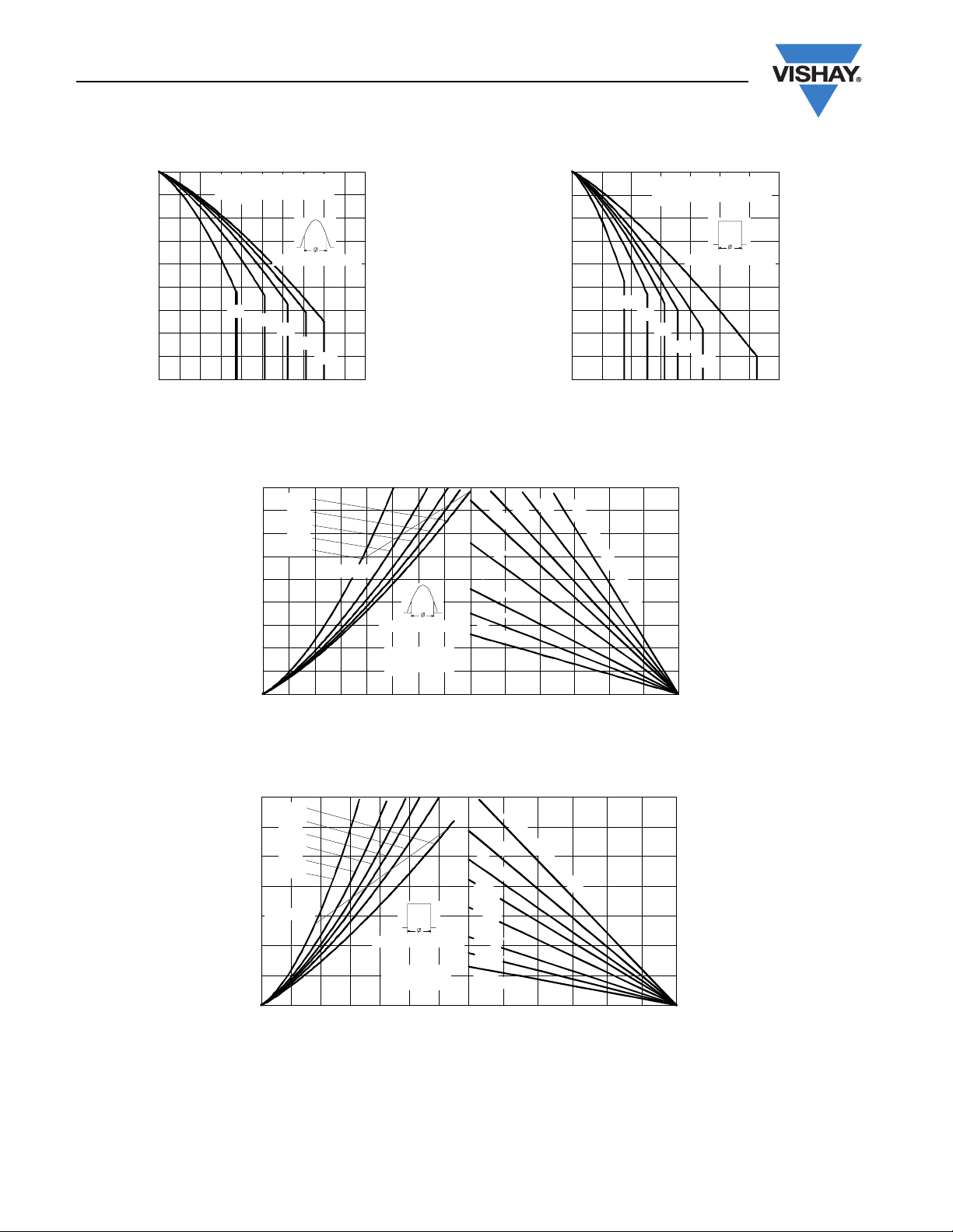
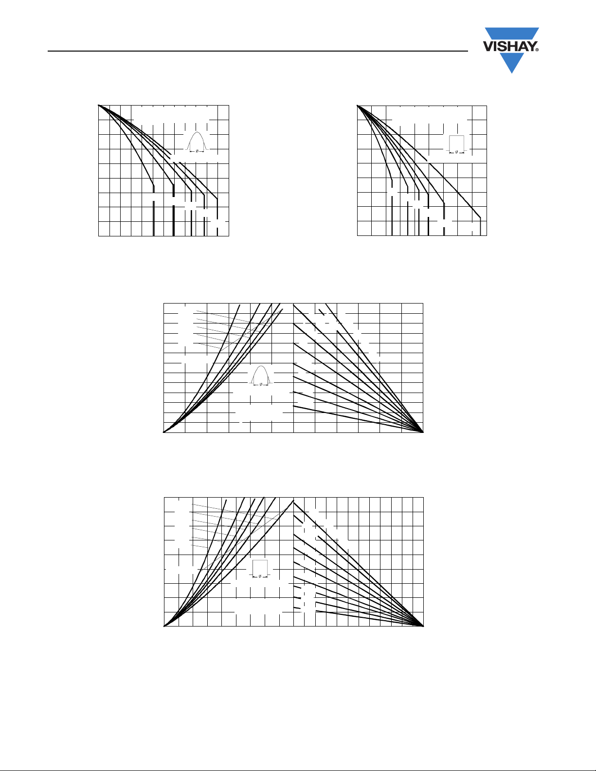
Fig. 1 - Current Ratings Characteristics Fig. 2 - Current Ratings Characteristics
Fig. 3 - Forward Power Loss Characteristics
Fig. 4 - Forward Power Loss Characteristics
60
70
80
90
100
110
120
130
140
150
01020304050
30°
60°
90°
120°
180°
Maximum Allowable Case Temperature (°C)
Cond uct ion Ang le
Av e ra g e Forwa rd Curre nt (A )
T4 0HF. . Se ri e s
R (DC) = 1.36 K/W
thJC
60
70
80
90
100
110
120
130
140
150
0 10203040506070
DC
30°
60°
90°
120°
180°
Maximum Allowable Case Temperature (°C)
Conduc tion Period
Average Forward Current (A)
T4 0H F. . Se r ie s
R (DC) = 1.36 K/W
thJC
0 255075100125150
Maximum Allowable Ambient Temperature (°C)
R
= 0
.
5
K
/
W
D
e
lt
a
R
thS
A
1
K
/
W
1
.
5
K
/
W
2
K
/
W
3
K
/
W
5
K
/
W
7
K
/
W
1
0
K
/
W
0
5
10
15
20
25
30
35
40
45
0 5 10 15 20 25 30 35 40
Average Forward Current (A)
RM S Li m it
Maximum Average Forward Power Loss (W)
Cond uction Angle
180°
120°
90°
60°
30°
T4 0 HF. . Se r i e s
T = 150°C
J
0255075100125150
Maximum Allowable Ambient Temperature (°C)
1
0
K
/
W
5
K
/
W
2
K
/
W
1
.
5
K
/
W
1
K
/
W
R
=
0
.
5
K
/
W
- D
e
l
t
a
R
t
h
S
A
7
K
/
W
3
K
/
W
0
10
20
30
40
50
60
70
0 10203040506070
DC
180°
120°
90°
60°
30°
RM S Lim it
Cond uc tion Period
Average Forward Current (A)
Maximum Average Forward Power Loss (W)
T40HF.. Series
T = 150°C
J

T40HF..., T70HF..., T85HF..., T110HF... Series
Power Rectifier Diodes
(T-Modules), 40 A to 110 A
Vishay Semiconductors
Fig. 5 - Maximum Non-Repetitive Surge Current
Fig. 6 - Maximum Non-Repetitive Surge Current
Fig. 7 - Current Ratings Characteristics
Fig. 8 - Current Ratings Characteristics
Fig. 9 - Forward Power Loss Characteristics
150
200
250
300
350
400
450
500
550
110100
Peak Half Sine Wave Forward Current (A)
Number Of Eq ual Amplitude Half Cycle Current Pulses (N)
Init ia l T = 150°C
@ 60 Hz 0.0083 s
@ 50 Hz 0.0100 s
At Any Ra ted Load Condition And With
Rated V Applied Following Surge.
J
RRM
T4 0 HF. . Se r i e s
100
150
200
250
300
350
400
450
500
550
600
0.01 0.1 1
Peak Half Sine Wave Forward Current (A)
Pulse Tra in Du ra ti o n ( s)
Maximum Non Repetitive Surge Current
T4 0HF. . Se ri e s
Initia l T = 150°C
No Voltage Reapplied
Ra t ed V Re a p p l i e d
RRM
Versus Pulse Train Duration.
J
60
70
80
90
100
110
120
130
140
150
0 1020304050607080
30°
60°
90°
120°
180°
Maximum Allowable Case Temp erature (°C)
Cond uct ion Ang le
Averag e Forwa rd Current (A)
T7 0 HF. . Se r i e s
R (DC) = 0.69 K/ W
thJC
60
70
80
90
100
110
120
130
140
150
020406080100120
DC
30°
60°
90°
120°
180°
Maximum Allowable Case Temperature (°C)
Conduction Period
Average Forwa rd Current (A)
T7 0H F. . Se r ie s
R (DC) = 0.69 K/W
thJC
0 25 50 75 100 125 150
Maximum Allowab le Ambient Temperature (°C)
R
=
0
.
3
K
/
W
D
e
l
t
a
R
t
h
S
A
0
.
5
K
/
W
0.7 K
/
W
1
K
/
W
1
.
5
K
/
W
2
K
/
W
3
K
/
W
5
K
/
W
7
K
/
W
0
10
20
30
40
50
60
70
80
90
0 10203040506070
Average Forward Current (A)
RM S Lim it
Maximum Average Forward Power Loss (W)
Cond uc tion Ang le
180°
120°
90°
60°
30°
T7 0H F. . Se ri e s
T = 150°C
J

T40HF..., T70HF..., T85HF..., T110HF... Series
Vishay Semiconductors
Power Rectifier Diodes
(T-Modules), 40 A to 110 A
Fig. 10 - Forward Power Loss Characteristics
Fig. 11 - Maximum Non-Repetitive Surge Current
Fig. 12 - Maximum Non-Repetitive Surge Current
Fig. 13 - Current Ratings Characteristics
Fig. 14 - Current Ratings Characteristics
0255075100125150
Maximum Allowable Ambient Temperature (°C)
0
.
5
K
/
W
0.
3
K
/W
0
.
7
K
/
W
1
K/
W
1
.
5
K
/
W
5
K
/
W
3
K
/
W
2
K
/
W
R
=
0
.
2
K
/
W
D
e
l
t
a
R
t
h
S
A
0
20
40
60
80
100
120
0 20406080100120
DC
180°
120°
90°
60°
30°
RM S Li m it
Conduction Period
Ave ra ge Forw a rd C urren t (A )
Maximum Average Forward Power Loss (W)
T7 0H F. . Se ri e s
T = 15 0 ° C
J
300
400
500
600
700
800
900
1000
1100
110100
Pea k Half Sine Wa ve Forw a rd C urren t ( A)
Number Of Equa l Amplitude Half Cycle Current Pulses (N)
T7 0 HF. . Series
Initial T = 150°C
@ 60 Hz 0.0083 s
@ 50 Hz 0.0100 s
At Any Rate d Loa d Co nd ition And With
Ra ted V App lied Fo llowing Surge .
J
RRM
200
300
400
500
600
700
800
900
1000
1100
1200
0.01 0.1 1
Peak Half Sine Wave Forward Current (A)
Pulse Train Duration (s)
Maximum Non Repet it ive Surge Current
T7 0 HF. . Se r i e s
Initial T = 150°C
No Vo ltag e Rea pp lied
Ra ted V Reap plied
RRM
Versus Pulse Train Duration.
J
80
90
100
110
120
130
140
150
0 102030405060708090
30°
60°
90°
120°
180°
Maximum Allo wable Case Temp erature (°C)
Cond uc tion Angle
Average Forward Current (A)
T8 5HF. . Se ri e s
R (DC) = 0.62 K/W
thJC
60
70
80
90
100
110
120
130
140
150
0 20 40 60 80 100 120 140
DC
30°
60°
90°
120°
180°
Maximum Allowable Case Temp erature (°C)
Cond uct ion Period
Average Forward Current (A)
T8 5H F. . Se r ie s
R (DC) = 0.62 K/W
thJC

T40HF..., T70HF..., T85HF..., T110HF... Series
Power Rectifier Diodes
(T-Modules), 40 A to 110 A
Vishay Semiconductors
Fig. 15 - Forward Power Loss Characteristics
Fig. 16 - Forward Power Loss Characteristics
Fig. 17 - Maximum Non-Repetitive Surge Current Fig. 18 - Maximum Non-Repetitive Surge Current
0 255075100125150
Maximum Allowable Ambient Temperature (°C)
R
=
0
.
2
K
/
W
D
e
l
t
a
R
t
h
S
A
0
.
3
K
/
W
0
.
5
K
/
W
0
.
7
K
/
W
1
K
/
W
1
.
5
K
/
W
2
K
/
W
3
K
/
W
5
K
/
W
7
K
/
W
0
10
20
30
40
50
60
70
80
90
100
0 102030405060708090
Average Forward Current (A)
RM S Lim i t
Maximum Average Forward Power Loss (W)
Cond uc tion A ngle
180°
120°
90°
60°
30°
T8 5H F. . Se r i e s
T = 1 50 ° C
J
0 25 50 75 100 125 150
Maximum Allowab le Ambient Temperature (°C)
0
.
5
K
/
W
0
.
3
K
/
W
0
.
7
K
/
W
1
K
/
W
1
.
5
K
/
W
2
K
/
W
3
K
/
W
5
K
/
W
R
=
0
.
2
K
/
W
D
e
l
t
a
R
t
h
S
A
0
20
40
60
80
100
120
140
0 20406080100120140
DC
180°
120°
90°
60°
30°
RM S Lim i t
Conduc tion Pe riod
Ave ra g e Forwa rd Cu rrent ( A)
Maximum Average Forward Power Loss (W)
T8 5 HF. . Se r i e s
T = 15 0° C
J
400
600
800
1000
1200
1400
1600
110100
Peak Half Sine Wave Forward Current (A)
Number Of Eq ual Amplitude Half Cycle Current Pulses (N)
T8 5HF. . Se r i e s
Init ia l T = 150°C
@ 60 Hz 0.0083 s
@ 50 Hz 0.0100 s
J
At Any Ra ted Load Condition And With
Rated V Applied Following Surge.
RRM
400
600
800
1000
1200
1400
1600
1800
0.01 0.1 1
Peak Half Sine Wave Forward Current (A)
Pulse Tra in Durat ion (s)
Maximum Non Repetitive Surge Current
Initial T = 150°C
No Vo lt a g e Rea p p lied
Rated V Reapp lied
J
Versus Pulse Train Dura tion.
RRM
T8 5 HF. . Se r i e s
T40HF..., T70HF..., T85HF..., T110HF... Series
Vishay Semiconductors
Power Rectifier Diodes
(T-Modules), 40 A to 110 A
Fig. 19 - Current Ratings Characteristics Fig. 20 - Current Ratings Characteristics
Fig. 21 - Forward Power Loss Characteristics
Fig. 22 - Forward Power Loss Characteristics
60
70
80
90
100
110
120
130
140
150
0 20406080100120
30°
60°
90°
120°
180°
Maximum Allowa ble Case Tem perature (°C)
Cond uc tion Ang le
Average Forward Current (A)
T1 1 0HF . . Series
R (DC) = 0.47 K/ W
thJC
60
70
80
90
100
110
120
130
140
150
0 20 40 60 80 100 120 140 160 180
DC
30°
60°
90°
120°
180°
Maximum Allowa ble Case Temperature (°C)
Conduc tion Period
T1 10 HF. . Se r i e s
R ( DC ) = 0. 47 K/ W
thJC
Average Forward Current (A)
0255075100125150
Maximum Allowa ble Amb ient Te mperature (°C)
5
K
/
W
3
K
/
W
2
K
/
W
1
.
5
K
/
W
1
K
/
W
0
.
7
K
/
W
0
.
5
K
/
W
0
.
3
K
/
W
R
=
0
.
2
K
/
W
D
e
l
t
a
R
t
h
S
A
0
10
20
30
40
50
60
70
80
90
100
110
120
130
0 20406080100120
Average Forward Current (A)
RM S Li m it
Ma ximum Avera ge Forwa rd Power Loss (W)
Cond uction A ngle
180°
120°
90°
60°
30°
T1 1 0HF. . Series
T = 15 0 ° C
J
0 25 50 75 100 125 150
Maximum Allow ab le Ambient Temp erature (°C)
5 K
/
W
3
K
/
W
2
K
/
W
1
.
5
K
/
W
1
K
/
W
0
.
7
K
/
W
0
.
5
K
/
W
0
.
3
K
/
W
R
=
0
.
2
K
/
W
D
e
l
t
a
R
t
h
S
A
0
20
40
60
80
100
120
140
160
180
0 20406080100120140160180
DC
180°
120°
90°
60°
30°
RM S Li m it
Cond uc tion Period
Average Forward Current (A)
Maximum Average Forward Power Loss ( W)
T1 1 0H F. . Series
T = 150°C
J

T40HF..., T70HF..., T85HF..., T110HF... Series
Power Rectifier Diodes
(T-Modules), 40 A to 110 A
Vishay Semiconductors
Fig. 23 - Maximum Non-Repetitive Surge Current
Fig. 24 - Maximum Non-Repetitive Surge Current
Fig. 25 - Forward Voltage Drop Characteristics
Fig. 26 - Forward Voltage Drop Characteristics
Fig. 27 - Forward Voltage Drop Characteristics
Fig. 28 - Forward Voltage Drop Characteristics
400
600
800
1000
1200
1400
1600
1800
110100
Peak Half Sine Wave Forw a rd C urre nt (A )
Num b er O f Equa l Amp litu d e Half Cy cle Cu rren t Pulses (N)
T1 1 0HF. . Se r i e s
Ini tia l T = 150° C
@ 60 Hz 0.0083 s
@ 50 Hz 0.0100 s
At Any Ra ted Load Condition And With
Ra ted V Ap p lied Fo llowing Surge.
RRM
J
400
600
800
1000
1200
1400
1600
1800
2000
0.01 0.1 1
Peak Half Sine Wave Forward Current (A)
Pulse Train Duration (s)
Maximum Non Repetitive Surge Current
T1 1 0H F. . Se r i e s
Initial T = 150°C
No Vo ltag e Rea pplied
Ra t e d V Re a p p l i e d
Ve rsus Pu lse Train Du ra t io n.
RRM
J
1
10
100
1000
00.511.522.533.54
T = 2 5 °C
J
Insta nta neo us Forw ard Cu rrent (A)
Instantaneous Forward Voltage (V)
T = 1 5 0° C
J
T4 0HF. . Se r ie s
1
10
100
1000
00.511.522.53
T = 25°C
J
Insta ntaneous Forward Current (A)
Instantaneous Forward Voltage (V)
T7 0H F. . Se ri e s
T = 1 50 ° C
J
10
100
1000
10000
012345
T = 2 5° C
J
In st a n t a n eo us Fo rw a rd C u rr e nt (A )
Instantaneous Forward Voltage (V)
T = 150°C
J
T8 5 HF. . Se ri e s
10
100
1000
10000
0 0.5 1 1.5 2 2.5 3 3.5 4 4.5 5
T = 25 ° C
J
Instantaneous Forward Current (A)
Instantaneous Forward Voltage (V)
T = 1 50 ° C
T1 10 HF. . Se r i e s
J

T40HF..., T70HF..., T85HF..., T110HF... Series
Vishay Semiconductors
Power Rectifier Diodes
(T-Modules), 40 A to 110 A
Fig. 29 - Thermal Impedance Z
thJC
Characteristics
ORDERING INFORMATION TABLE
0.01
0.1
1
10
0.0001 0.001 0.01 0.1 1 10 100
Sq uare Wave Pulse Durat ion ( s)
thJC
Transient Thermal Impedance Z (K/W)
St e a d y St a t e V a lu e :
R = 1.36 K/ W
R = 0.69 K/ W
R = 0.62 K/ W
R = 0.47 K/ W
(DC Operation)
thJC
thJC
thJC
thJC
T4 0HF. . Se ri e s
T7 0 HF. . Series
T8 5H F. . Se ri e s
T1 10 H F. . Se r ie s
CIRCUIT CONFIGURATION
CIRCUIT DESCRIPTION
CIRCUIT
CONFIGURATION CODE
CIRCUIT DRAWING
Single diode HF
1
- Module type
3
- Circuit configuration (see Circuit Configuration table)
- Voltage code x 10 = V
RRM
4
- Current rating
2
Device code
1324
T 110 HF 120
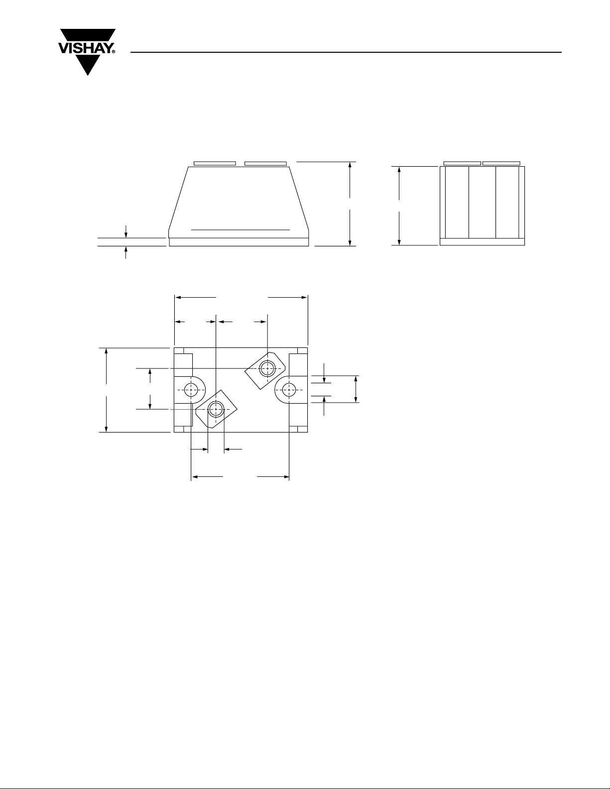
D-55 T-Module Diode Standard and Fast Recovery
DIMENSIONS in millimeters (inches)
Outline Dimensions
Vishay High Power Products
3 (0.12)
27 (1.06)
15 (0.59)
-
11
(0.43)
41 (1.61) MAX.
18
(0.71)
M5
30 (1.18)
+
3.9 (0.15)
25 ± 1
23.5 (0.93)
8 (0.31)

Disclaimer
Legal Disclaimer Notice
Vishay
All product specifications and data are subject to change without notice.
Vishay Intertechnology, Inc., its affiliates, agents, and employees, and all persons acting on its or their behalf
(collectively, “Vishay”), disclaim any and all liability for any errors, inaccuracies or incompleteness contained herein
or in any other disclosure relating to any product.
Vishay disclaims any and all liability arising out of the use or application of any product described herein or of any
information provided herein to the maximum extent permitted by law. The product specifications do not expand or
otherwise modify Vishay’s terms and conditions of purchase, including but not limited to the warranty expressed
therein, which apply to these products.
No license, express or implied, by estoppel or otherwise, to any intellectual property rights is granted by this
document or by any conduct of Vishay.
The products shown herein are not designed for use in medical, life-saving, or life-sustaining applications unless
otherwise expressly indicated. Customers using or selling Vishay products not expressly indicated for use in such
applications do so entirely at their own risk and agree to fully indemnify Vishay for any damages arising or resulting
from such use or sale. Please contact authorized Vishay personnel to obtain written terms and conditions regarding
products designed for such applications.
Product names and markings noted herein may be trademarks of their respective owners.
 Loading...