

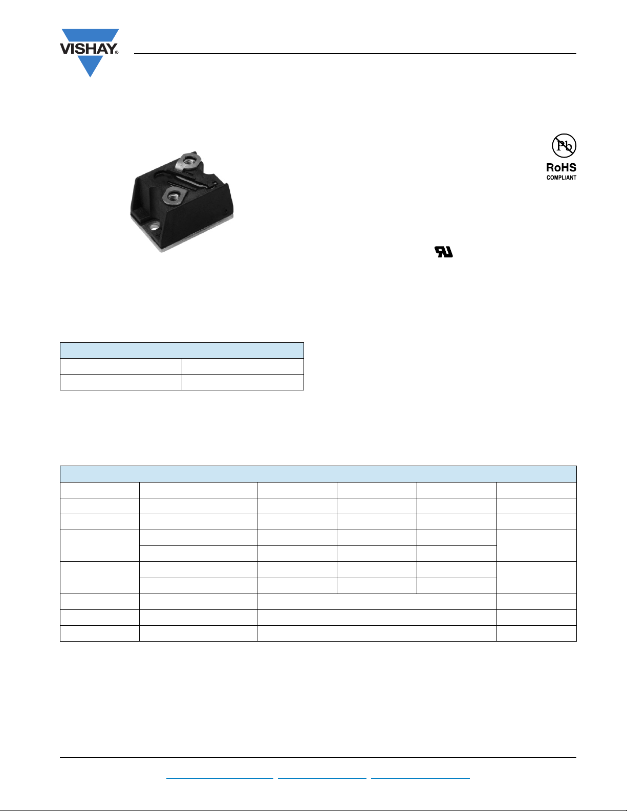
Fast Recovery Diodes (T-Modules), 40 A/70 A/85 A
PRODUCT SUMMARY
I
F(AV)
Type Modules - Diode, Fast
D-55
40 A/70 A/85 A
T40HFL, T70HFL, T85HFL Series
Vishay Semiconductors
FEATURES
• Fast recovery time characteristics
• Electrically isolated base plate
• 3500 V
• Standard JEDEC package
• Simplified mechanical designs, rapid assembly
• Large creepage distances
• UL E78996 approved
• Compliant to RoHS directive 2002/95/EC
• Designed and qualified for industrial level
DESCRIPTION
The series of T-modules uses fast recovery power diodes in
a single diode configuration. The semiconductors are
electrically isolated from the metal base, allowing common
heatsink and compact assemblies to be built.
These single diode modules can be used in conjunction with
the thyristor modules as a freewheel diode. Application
includes self-commutated inverters, DC choppers, motor
control, inductive heating and electronic welders. These
modules are intended for those applications where very fast
recovery characteristics are required and for general power
switching applications.
isolating voltage
RMS
MAJOR RATINGS AND CHARACTERISTICS
SYMBOL CHARACTERISTICS T40HFL T70HFL T85HFL UNITS
I
F(AV)
I
F(RMS)
I
FSM
2
I
t
V
RRM
t
rr
T
J
Document Number: 93184 For technical questions within your region, please contact one of the following: www.vishay.com
Revision: 19-May-10 DiodesAmericas@vishay.com
50 Hz 475 830 1300
60 Hz 500 870 1370
50 Hz 1130 3460 8550
60 Hz 1030 3160 7810
Range 100 to 1000 V
Range 200 to 1000 ns
Range - 40 to 125 °C
40 70 85 A
63 110 133 A
A
A2s
, DiodesAsia@vishay.com, DiodesEurope@vishay.com 1
T40HFL, T70HFL, T85HFL Series
Vishay Semiconductors
Fast Recovery Diodes
(T-Modules), 40 A/70 A/85 A
ELECTRICAL SPECIFICATIONS
VOLTAGE RATINGS
V
, MAXIMUM
V
MAXIMUM REPETITIVE
TYPE NUMBER
VOLTAGE
CODE
t
rr
CODE
RRM,
PEAK REVERSE VOLTAGE
V
10 S02, S05, S10 100 150
20 S02, S05, S10 200 300
T40HFL..
T70HFL..
T85HFL..
40 S02, S05, S10 400 500
60 S02, S05, S10 600 700
80 S05, S10 800 900
100 S05, S10 1000 1100
FORWARD CONDUCTION
PARAMETER SYMBOL TEST CONDITIONS T40HFL T70HFL T85HFL UNITS
Maximum average
forward current
at case temperature
Maximum RMS
forward current
Maximum peak, one-cycle
forward, non-repetitive
surge current
Maximum I
Maximum I
2
t for fusing I2t
2
√t for fusing I2√t t = 0.1 ms to 10 ms, no voltage reapplied 11 300 34 600 85 500 A2√s
Low level value of
threshold voltage
High level value of
threshold voltage
Low level value of forward
slope resistance
High level value of forward
slope resistance
Maximum forward
voltage drop
I
F(AV)
I
F(RMS)
I
FSM
V
F(TO)1
V
F(TO)2
r
r
V
180° conduction, half sine wave
t = 10 ms
t = 8.3 ms 500 870 1370
t = 10 ms
t = 8.3 ms 420 730 1150
t = 10 ms
t = 8.3 ms 1030 3160 7810
t = 10 ms
t = 8.3 ms 730 2230 5520
TJ = 25 °C, (16.7 % x π x I
TJ = 25 °C, (I > π x I
TJ = 25 °C, (16.7 % x π x I
f1
TJ = 25 °C, (I > π x I
f2
IFM = π x I
FM
Average power = V
No voltage
reapplied
100 % V
RRM
reapplied
No voltage
Sinusoidal half wave,
initial T
= TJ maximum
J
reapplied
100 % V
RRM
reapplied
< I < π x I
F(AV)
) 0.84 0.90 0.86
F(AV)
< I < π x I
F(AV)
) 6.8 2.67 2.07
F(AV)
, TJ = 25 °C, tp = 400 μs square wave
F(AV)
F(TO)
x I
F(AV)
+ rf x (I
F(AV)
F(AV)
F(RMS)
RSM
NON-REPETITIVE PEAK
REVERSE VOLTAGE
I
RRM
AT T
V
40 70 85 A
70 °C
63 110 133 A
475 830 1300
400 700 1100
1130 3460 8550
800 2450 6050
) 0.82 0.87 0.84
) 7.0 2.77 2.15
2
)
1.60 1.73 1.55 V
MAXIMUM
= 25 °C
J
μA
100
A
A
V
mΩ
2
s
www.vishay.com For technical questions within your region, please contact one of the following: Document Number: 93184
2 DiodesAmericas@vishay.com
, DiodesAsia@vishay.com, DiodesEurope@vishay.com Revision: 19-May-10
T40HFL, T70HFL, T85HFL Series
Fast Recovery Diodes
Vishay Semiconductors
(T-Modules), 40 A/70 A/85 A
REVERSE RECOVERY CHARACTERISTICS
PARAMETER SYMBOL TEST CONDITIONS
(1)
TJ = 25 °C, -dIF/dt = 100 A/μs
I
Maximum reverse
recovery time
t
rr
= 1 A to VR = 30 V
F
= 25 °C, -dIF/dt = 25 A/μs
T
J
= π x rated I
I
FM
, VR = - 30 V
F(AV)
TJ = 25 °C, -dIF/dt = 100 A/μs
= 1 A to VR = 30 V
Maximum reverse
recovery charge
Q
I
F
rr
= 25 °C, -dIF/dt = 25 A/μs
T
J
I
= π x rated I
FM
, VR = - 30 V
F(AV)
Note
(1)
Tested on LEM 300 A diodemeter tester
BLOCKING
PARAMETER SYMBOL TEST CONDITIONS T40HFL T70HFL T85HFL UNITS
Maximum peak reverse leakage current I
RMS isolation voltage V
RRM
ISOL
T40HFL T70HFL T85HFL
S02 S05 S10 S02 S05 S10 S02 S05 S10
70 110 270 70 110 270 80 120 290
200 500 1000 200 500 1000 200 500 1000
0.25 0.4 1.35 0.25 0.4 1.35 0.3 0.6 1.6
0.55 2.0 8.0 0.6 2.1 8.5 0.8 3.5 1.5
TJ = 125 °C 20 mA
50 Hz, circuit to base, all terminals
shorted, T
= 25 °C, t = 1 s
J
3500 V
UNITS
ns
μC
THERMAL AND MECHANICAL SPECIFICATIONS
PARAMETER SYMBOL TEST CONDITIONS T40HFL T70HFL T85HFL UNITS
Junction operating temperature range T
Storage temperature range T
Maximum internal thermal resistance,
junction to case per module
Thermal resistance,
case to heatsink per module
R
R
base to heatsink
Mounting torque ± 10 %
busbar to terminal
Approximate weight
J
Stg
thJC
thCS
DC operation 0.85 0.53 0.46
Mounting surface, flat, smooth
and greased
M3.5 mounting screws
(1)
Non-lubricated threads
M5 screws terminals
Non-lubricated threads
See dimensions link at the end of datasheet
- 40 to 125
- 40 to 150
0.2
1.3 ± 10 %
3 ± 10 %
54 g
19 oz.
°C
K/W
Nm
Case style D-55 (T-module)
Note
(1)
A mounting compound is recommended and the torque should be rechecked after a period of about 3 hours to allow for the spread of
the compound
ΔR CONDUCTION
DEVICES
SINUSOIDAL CONDUCTION AT T
180° 120° 90° 60° 30° 180° 120° 90° 60° 30°
T40HFL 0.06 0.08 0.10 0.14 0.24 0.05 0.08 0.10 0.15 0.24
T85HFL 0.04 0.05 0.06 0.09 0.15 0.03 0.05 0.07 0.09 0.015
Note
• The table above shows the increment of thermal resistance R
Document Number: 93184 For technical questions within your region, please contact one of the following: www.vishay.com
Revision: 19-May-10 DiodesAmericas@vishay.com
MAXIMUM RECTANGULAR CONDUCTION AT TJ MAXIMUM
J
UNITS
K/WT70HFL 0.05 0.06 0.08 0.11 0.19 0.04 0.06 0.08 0.12 0.19
when devices operate at different conduction angles than DC
thJC
, DiodesAsia@vishay.com, DiodesEurope@vishay.com 3
T40HFL, T70HFL, T85HFL Series
Vishay Semiconductors
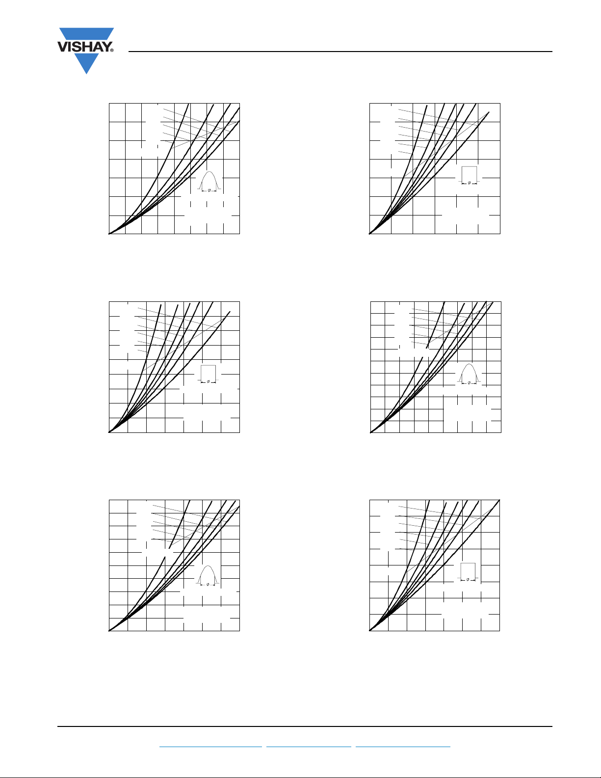
130
120
110
100
90
80
70
60
50
0 1020304050
Maximum Allowable Case Temperature (°C)
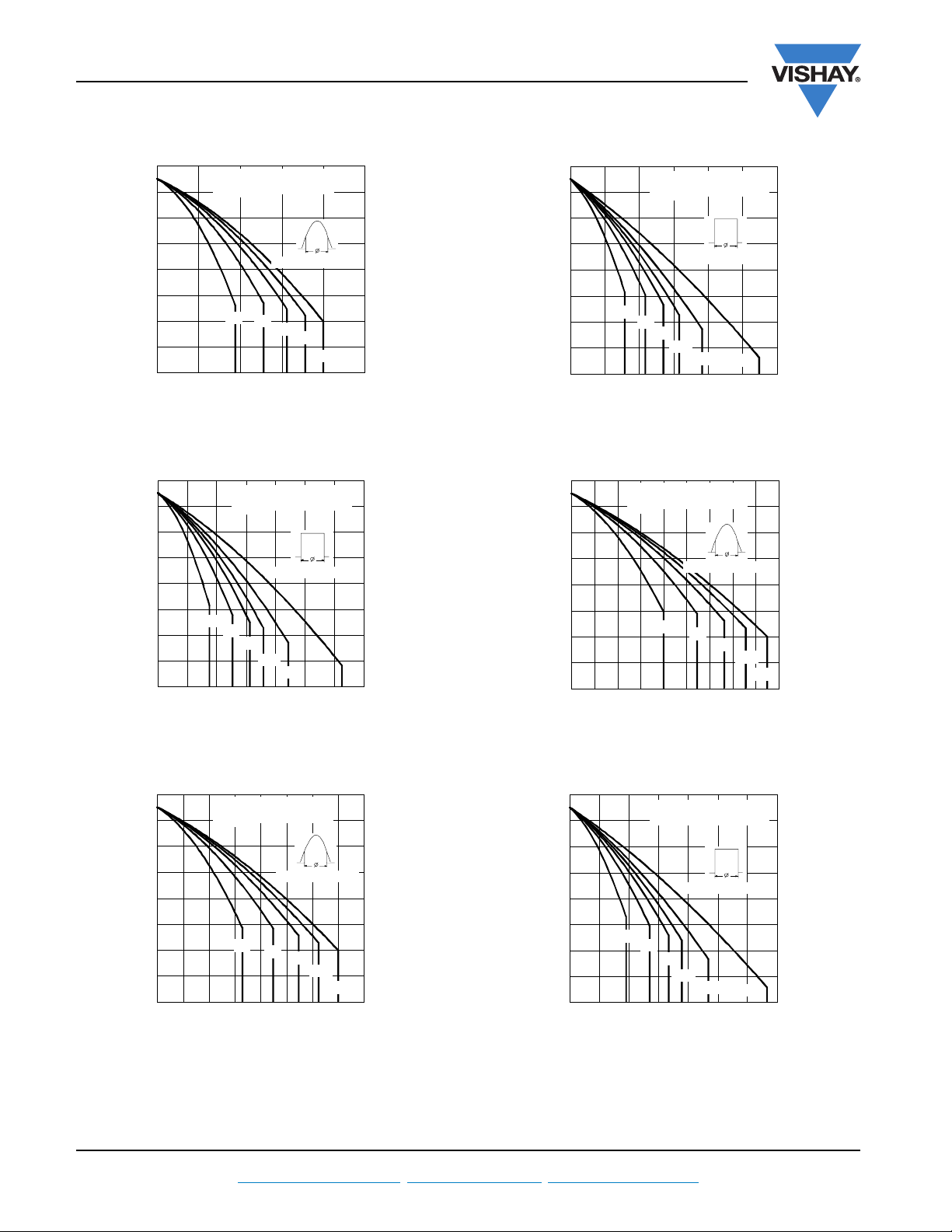
Fig. 1 - Current Ratings Characteristics
130
120
110
100
90
80
70
60
50
0 10203040506070
Maximum Allowable Case Temperature (°C)
Fig. 2 - Current Ratings Characteristics
T4 0H FL. . Se r ie s
R (DC) = 0.85 K/W
thJC
Conduct ion Angle
30°
60°
90°
Average Forward Current (A)
T4 0HFL. . Se ri e s
R (DC) = 0.85 K/W
thJC
Cond uc tion Period
30°
60°
90°
120°
180°
Average Fo rward Current (A)
120°
Fast Recovery Diodes
(T-Modules), 40 A/70 A/85 A
180°
DC
130
120
110
100
90
80
70
60
50
Maxim um Allowa ble Case Temperature (°C)
0 20406080100120
Average Forward Current (A)
T7 0H FL. . Se ri e s
R (DC) = 0.53 K/ W
thJC
Conduction Period
30°
60°
90°
120°
180°
Fig. 4 - Current Ratings Characteristics
130
120
110
100
90
80
70
60
50
Maximum Allowable Case Temperature (°C)
0 102030405060708090
T8 5H FL. . Se r i e s
R (DC) = 0.46 K/W
thJC
Conduction Angle
30°
60°
90°
Avera ge Forwa rd Current (A)
Fig. 5 - Current Ratings Characteristics
DC
120°
180°
130
120
110
100
90
80
70
60
50
Maximum Allow able Case Temperature (°C)
0 1020304050607080
T7 0HFL . . Se ri e s
R (D C) = 0 .5 3 K/ W
thJC
Cond uct io n Angle
30°
60°
90°
Average Forward Current (A)
Fig. 3 - Current Ratings Characteristics
120°
180°
130
120
110
100
90
80
70
60
50
Maximum Allowable Case Temperature (°C)
020406080100120140
Average Forward Current (A)
T8 5H FL. . Se r i e s
R ( DC ) = 0. 46 K/ W
thJC
Conduction Period
30°
60°
90°
120°
180°
Fig. 6 - Current Ratings Characteristics
DC
www.vishay.com For technical questions within your region, please contact one of the following: Document Number: 93184
4 DiodesAmericas@vishay.com
, DiodesAsia@vishay.com, DiodesEurope@vishay.com Revision: 19-May-10
T40HFL, T70HFL, T85HFL Series
70
60
50
40
30
20
10
0
0 5 10 15 20 25 30 35 40
Maximum Average Forward Power Lo ss (W)
180°
120°
90°
60°
30°
RM S Lim it
Conduc tion Angle
T4 0HFL .. Se ri e s
T = 12 5 ° C
J
Average Forward Current (A)
Fig. 7 - Forward Power Loss Characteristics
90
DC
80
180°
120°
70
90°
60°
60
30°
50
RM S Lim it
40
30
20
10
0
0 10203040506070
Maximum Averag e Forward Power Lo ss (W)
Average Forward Current (A)
Conduct ion Period
T4 0H FL. . Se r ie s
T = 125°C
J
Fig. 8 - Forward Power Loss Characteristics
Fast Recovery Diodes
(T-Modules), 40 A/70 A/85 A
140
120
100
80
60
40
20
0
Maximum Average Forward Power Loss (W)
020406080100120
Fig. 10 - Forward Power Loss Characteristics
110
100
90
80
70
60
50
40
30
20
10
0
Maximum Average Forward Power Loss (W)
0 102030405060708090
Fig. 11 - Forward Power Loss Characteristics
Vishay Semiconductors
DC
180°
120°
90°
60°
30°
RM S Li m it
Cond uc tion Period
T70HFL.. Series
T = 1 25 ° C
Av e ra g e Fo rwa rd Curre nt (A)
180°
120°
90°
60°
30°
RM S Lim it
Conduction Angle
T85HFL.. Series
T = 125°C
Average Forward Current (A)
J
J
100
90
80
70
60
50
40
30
20
10
0
Maximum Average Forward Power Loss (W)
180°
120°
90°
60°
30°
RM S Lim it
Conduction Angle
T7 0H FL. . Se r ie s
T = 125° C
J
0 10203040506070
Average Forward Current (A)
Fig. 9 - Forward Power Loss Characteristics
160
DC
180°
140
120°
90°
120
60°
30°
100
80
RM S Li m it
60
40
20
0
Maximum Average Forward Power Loss (W)
0 20 40 60 80 100 120 140
Average Forward Current (A)
Conduction Perio d
T85HFL.. Series
T = 1 25 °C
J
Fig. 12 - Forward Power Loss Characteristics
Document Number: 93184 For technical questions within your region, please contact one of the following: www.vishay.com
Revision: 19-May-10 DiodesAmericas@vishay.com
, DiodesAsia@vishay.com, DiodesEurope@vishay.com 5

T40HFL, T70HFL, T85HFL Series
Vishay Semiconductors
450
At Any Rated Load Condition And With
Ra t e d V A p p l ie d Fo ll o w in g Su r g e .
400
350
300
250
200
150
T4 0HF L . . Se r i e s
100
Pe ak Ha lf Sine Wave Fo rwa rd Current (A)
110100
Number Of Equal Amplitude Half Cycle Current Pulses (N)
Fig. 13 - Maximum Non-Repetitive Surge Current
500
Maxim um Non Repe t itive Su rge Current
450
400
350
300
250
200
150
T4 0H FL. . Se ri e s
100
Peak Half Sine Wave Forward Current (A)
0.01 0.1 1
RRM
Versus Pulse Tra in Duration.
Pulse Train Duration (s)
Init ial T = 125°C
@ 60 Hz 0.0083 s
@ 50 Hz 0.0100 s
Init ia l T = 125° C
No Vo ltage Rea p p lie d
Ra t e d V Re a p p l ie d
RRM
Fast Recovery Diodes
(T-Modules), 40 A/70 A/85 A
J
J
850
Maximum Non Repetitive Surge Current
750
650
550
450
350
250
Pea k Half Sin e Wa ve Forw a rd Curre nt (A )
150
0.01 0.1 1
Versus Pulse Train Dura tion.
No Vo lt a g e Rea pplied
Rat ed V Rea ppl ied
T7 0H FL . . Se ri e s
Pulse Tra in Durat ion (s)
Initia l T = 125°C
J
RRM
Fig. 16 - Maximum Non-Repetitive Surge Current
1200
1100
1000
Pea k Half Sine Wave Forwa rd Current (A)
At Any Rate d Lo a d Co nd ition And With
Ra ted V Ap p lied Fo llowing Surge.
RRM
900
800
700
600
500
T85HFL.. Series
400
300
110100
Numbe r Of Equal Am plitud e Half Cyc le Current Pulses (N)
Ini tia l T = 125° C
J
@ 60 Hz 0.0083 s
@ 50 Hz 0.0100 s
Fig. 14 - Maximum Non-Repetitive Surge Current
800
At Any Rated Loa d Cond ition And With
Rated V Applied Following Surge.
700
600
500
400
300
T70HFL.. Series
Peak Half Sine Wave Forw ard C urrent (A)
200
110100
Number Of Eq ual Amplitude Half Cycle Current Pulses (N)
RRM
Initia l T = 125°C
J
@ 60 Hz 0.0083 s
@ 50 Hz 0.0100 s
Fig. 15 - Maximum Non-Repetitive Surge Current
Fig. 17 - Maximum Non-Repetitive Surge Current
1300
Ma ximum Non Repet itive Surge Current
1200
1100
1000
900
800
700
600
500
400
Peak Half Sine Wave Forward Current (A)
300
0.01 0 .1 1
Versus Pulse Train Duration.
No Vo lt ag e Rea p plied
Rated V Reapplied
T8 5HF L . . Se ri e s
Pulse Train Duration (s)
Init ial T = 125°C
J
RRM
Fig. 18 - Maximum Non-Repetitive Surge Current
www.vishay.com For technical questions within your region, please contact one of the following: Document Number: 93184
6 DiodesAmericas@vishay.com
, DiodesAsia@vishay.com, DiodesEurope@vishay.com Revision: 19-May-10

T40HFL, T70HFL, T85HFL Series
(T-Modules), 40 A/70 A/85 A
0.51
0.5
I = 300A
50A
T4 0 H F L . . S0 2
T7 0 H F L . . S0 2
T = 12 5 ° C
FM
220A
172A
100A
50A
00101
J
0.49
0.48
0.47
T4 0 H FL. . S0 2
0.46
T7 0 H FL. . S0 2
T = 1 2 5 ° C
Maximum Reverse Recovery Time - Trr (µs)
Ra te Of Fall Of Fo rwa rd Current - di/ dt (A/ µs)
J
0.45
Fig. 19 - Recovery Time Characteristics
8
I = 300A
FM
220A
7
6
5
4
3
2
1
10 20 30 40 50 60 70 80 90 100
Ma ximu m Reverse Rec ov e ry Ch arg e - Q rr (µC )
Ra te Of Fa ll Of Forward Current - di/d t (A/µs)
172A
100A
Fast Recovery Diodes
Vishay Semiconductors
1.1
1
I = 300A
FM
0.9
0.8
0.7
T4 0 HF L . . S0 5
T7 0 HF L . . S0 5
T = 1 2 5 ° C
J
Maximum Reverse Recovery Time - Trr (µs)
0.6
Rate Of Fall Of Forward Current - di/dt (A/µs)
Fig. 22 - Recovery Time Characteristics
20
I = 3 00A
FM
18
16
14
12
10
8
6
4
10 20 30 40 50 60 70 80 90 100
Maximum Reverse Recovery Charge - Qrr (µC)
Ra te O f Fa ll Of Forwa rd Curre nt - di/ dt (A/ µs)
220A
172A
100A
50A
220A
172A
100A
50A
T4 0 H FL . . S0 5
T7 0 H FL . . S0 5
T = 12 5 ° C
J
00101
Fig. 20 - Recovery Charge Characteristics
20
I = 300A
FM
18
16
14
12
10
8
6
4
Maximum Reverse Recovery Current - Irr (A)
Ra te Of Fa ll Of Forward Current - di/dt (A/ µs)
220A
172A
100A
50A
T4 0 HF L . . S0 2
T7 0 HF L . . S0 2
T = 1 2 5 ° C
J
10 20 30 40 50 60 70 80 90 100
Fig. 21 - Recovery Current Characteristics
Fig. 23 - Recovery Charge Characteristics
28
26
I = 3 00A
FM
24
22
20
18
16
14
12
10
8
6
M a xim um Reve rse Rec o ve ry C urre nt - Irr ( A)
Rate Of Fall Of Forward Current - di/dt (A/ µs)
220A
172A
100A
50A
T4 0 H F L . . S0 5
T7 0 H F L . . S0 5
T = 125 °C
J
10 20 30 40 50 60 70 80 90 100
Fig. 24 - Recovery Current Characteristics
Document Number: 93184 For technical questions within your region, please contact one of the following: www.vishay.com
Revision: 19-May-10 DiodesAmericas@vishay.com
, DiodesAsia@vishay.com, DiodesEurope@vishay.com 7

T40HFL, T70HFL, T85HFL Series
Vishay Semiconductors
1.8
1.7
1.6
1.5
1.4
1.3
1.2
T4 0 H F L . . S1 0
T7 0 H F L . . S1 0
1.1
T = 125 °C
J
Maximum Reverse Rec overy Time - Trr (µs)
1
Ra te Of Fa ll Of Forward Current - di/d t (A/µs)
Fig. 25 - Recovery Time Characteristics
40
35
30
25
20
100A
50A
I = 300A
FM
I = 300A
200A
Fast Recovery Diodes
(T-Modules), 40 A/70 A/85 A
1.2
FM
00101
200A
100A
50A
1.1
1
0.9
0.8
T8 5 H FL . . S0 2
0.7
T = 1 2 5° C
J
Ma xim um Re verse Rec ove ry Time - Trr ( µs)
0.6
Ra te Of Fall Of Forward C urrent - di/dt (A/µs)
I = 300A
FM
200A
100A
50A
00101
Fig. 28 - Recovery Time Characteristics
25
I = 300A
FM
20
15
200A
100A
50A
15
10
5
10 20 30 40 50 60 70 80 90 100
Maximum Reverse Re covery Cha rge - Qrr (µC)
Ra te Of Fall O f Forw ard Current - d i/ d t (A/ µs)
T4 0 HF L . . S1 0
T7 0 HF L . . S1 0
T = 1 2 5 ° C
J
Fig. 26 - Recovery Charge Characteristics
45
40
35
30
25
20
15
10
Maximum Reverse Rec overy Current - Irr (A)
10 20 30 40 50 60 70 80 90 100
Ra te Of Fall Of Fo rwa rd Current - di/ dt (A/µs)
I = 300A
FM
T4 0 H FL . . S1 0
T7 0 H FL . . S1 0
T = 12 5 ° C
J
200A
100A
50A
Fig. 27 - Recovery Current Characteristics
10
T8 5 H F L . . S0 2
T = 1 2 5 ° C
5
10 20 30 40 50 60 70 80 90 100
Maximum Reverse Recovery Charge - Qrr (µC)
Ra te Of Fall Of Forward Current - di/dt (A/ µs)
J
Fig. 29 - Recovery Charge Characteristics
28
I = 300A
FM
26
24
22
20
18
16
14
12
10
8
6
Ma ximum Re verse Rec ov e ry Cu rren t - Irr (A )
10 20 30 40 50 60 70 80 90 100
Ra t e O f Fa ll O f Fo rw a rd C ur re n t - d i / d t ( A / µs)
200A
100A
50A
T8 5 H FL. . S0 2
T = 125°C
J
Fig. 30 - Recovery Current Characteristics
www.vishay.com For technical questions within your region, please contact one of the following: Document Number: 93184
8 DiodesAmericas@vishay.com
, DiodesAsia@vishay.com, DiodesEurope@vishay.com Revision: 19-May-10

T40HFL, T70HFL, T85HFL Series
(T-Modules), 40 A/70 A/85 A
1.3
1.2
I = 300A
1.1
1
0.9
T8 5 H FL . . S0 5
T = 12 5 °C
J
Ma ximum Reverse Rec ove ry Tim e - Trr ( µs)
0.8
Ra te Of Fall Of Forward Current - di/d t (A/µs)
Fig. 31 - Recovery Time Characteristics
30
27
24
21
18
15
12
9
6
10 20 30 40 50 60 70 80 90 100
Maximum Reverse Recovery Charge - Qrr (µC)
Ra t e O f Fa l l Of Fo r wa r d C u rr en t - d i / d t (A / µ s)
Fig. 32 - Recovery Charge Characteristics
FM
200A
100A
I = 300A
FM
200A
100A
T8 5 H FL . . S0 5
T = 12 5° C
J
50A
00101
50A
Fast Recovery Diodes
Vishay Semiconductors
2
1.9
1.8
1.7
1.6
1.5
1.4
1.3
1.2
T8 5 H F L . . S1 0
1.1
T = 125°C
J
Maximum Reverse Recovery Time - Trr (µs)
1
Rate Of Fall Of Forward Current - di/dt (A/ µs)
Fig. 34 - Recovery Time Characteristics
55
50
45
40
35
30
25
20
15
10
10 20 30 40 50 60 70 80 90 100
Maximum Reverse Recovery Charge - Qrr (µC)
Ra te Of Fa ll Of Forward Current - di/dt (A/ µs)
Fig. 35 - Recovery Charge Characteristics
I = 300A
FM
I = 300A
FM
T8 5 H F L . . S1 0
T = 125°C
J
200A
100A
50A
00101
200A
100A
50A
35
30
25
20
15
10
Ma ximum Reve rse Re co ve ry C urrent - Irr (A)
10 20 30 40 50 60 70 80 90 10 0
Ra t e O f Fa ll O f For w a rd C u r re n t - d i / d t ( A/ µ s)
I = 300A
FM
200A
T8 5 H FL . . S0 5
T = 125° C
J
100A
50A
Fig. 33 - Recovery Current Characteristics
60
55
50
45
40
35
30
25
20
15
Ma ximu m Reve rse Re c overy Curren t - Irr (A)
10 20 30 40 50 60 70 80 90 100
Rate Of Fall Of Forward Current - di/dt (A/µs)
I = 300A
FM
T8 5 H F L . . S1 0
T = 125°C
J
200A
100A
50A
Fig. 36 - Recovery Current Characteristics
Document Number: 93184 For technical questions within your region, please contact one of the following: www.vishay.com
Revision: 19-May-10 DiodesAmericas@vishay.com
, DiodesAsia@vishay.com, DiodesEurope@vishay.com 9

T40HFL, T70HFL, T85HFL Series
4
4
Vishay Semiconductors
1E4
1E3
20000
1E2
Peak Forw ard Current (A)
1E1
1E1 1E2 1E3 1E
10000
tp
T4 0H FL .. Se r i e s
Si n u so i d a l P u l se
T = 70°C
1E4
1E3
2500
5000
C
Pu lse Ba se w id t h ( µ s)
Fast Recovery Diodes
(T-Modules), 40 A/70 A/85 A
1500
1000
400
Fig. 37 - Frequency Characteristics
200
50 Hz
1E1
1E4
E1 1E2 1E3 1 E4
T4 0H FL. . Series
Tr a p e zo i d a l Pu l se
T = 70 °C
tp
T4 0 H F L. .
Tr a p e zo i d a l Pu l se
T = 9 0 °C
tp
C
C
2500
5000
1500
Pulse Base w id th (µ s)
1000
400
200
50 Hz
1E2
Peak Forward Current (A)
1E1
1E1 1E2 1E3 1E4
tp
1000020000
5000
T40HFL.. Serie s
Si n u so i d a l Pu l se
T = 90°C
C
15002500
200
Pulse Basewidth (µs)
Fig. 38 - Frequency Characteristics
1E4
20 joule s p er pulse
10
1E3
0.1
0.04
1E2
1E1
Peak Forward Current (A)
tp
1E0
1E1 1E2 1E3 1E
0.02
0.01
T40HFL.. Serie s
Sin usoid al Pulse
T = 125 °C
J
4
2
1
0.4
0.2
Pulse Basewidth (µs)
Fig. 39 - Maximum Forward Energy Power Loss Characteristics
50 Hz4001000
1E1
1E4
E1 1 E2 1 E3 1 E4
5000
2500
1500
1000
400
Pu lse Ba sew id t h ( µ s)
10
4
2
1
0.4
0.2
0.1
0.04
0.02
0.01
T40HFL.. Seri es
Tr a p e z o i d a l P u ls e
T = 125°C
J
tp
di/dt = 50A/µs
1E4
E1 1 E2 1 E3 1 E4
1E1
Pu l se Ba sew id t h (µ s)
200
50 Hz
20 joules pe r pu lse
www.vishay.com For technical questions within your region, please contact one of the following: Document Number: 93184
10 DiodesAmericas@vishay.com
, DiodesAsia@vishay.com, DiodesEurope@vishay.com Revision: 19-May-10

T40HFL, T70HFL, T85HFL Series
Fast Recovery Diodes
(T-Modules), 40 A/70 A/85 A
1E4
1E3
5000
1000020000
1E2
tp
T70 HFL. . Se ri e s
Sinu so id al Pul se
T = 70 ° C
C
Peak Forward Current (A)
1E1
1 E1 1 E2 1 E3 1 E4
Pulse Ba se w id t h ( µ s)
1E4
1E3
2500
1500
1000
400
200
Fig. 40 - Frequency Characteristics
Vishay Semiconductors
50 Hz
tp
1E1 1E2 1E3 1E4
1E1
1E4
5000
T70HFL.. Series
Tr a p e zo i d a l Pu l se
T = 70°C
C
2500
1500
Pu lse Ba se w id t h (µ s)
400
1000 200
50 Hz
10000
5000
20000
1E2
tp
T7 0H FL . . S e ri e s
Sinusoida l Pulse
T = 90°C
Pe ak Fo rw a rd C urr e n t ( A)
1E1
1E1 1E2 1E3 1E4
2500
1500
C
4001000
200
Pu l se Ba se w i d t h ( µ s)
Fig. 41 - Frequency Characteristics
1E4
20 joules p er pulse
10
4
1E3
0.04
1E2
1E1
Peak Forward Current (A)
1E0
tp
1E1 1E2 1E3 1E4
0.02
0.01
T7 0H FL . . Se r i e s
Si n u so i d a l Pu l se
T = 125°C
J
2
1
0.4
0.2
0.1
Pu lse Ba se w id t h ( µ s)
Fig. 42 - Maximum Forward Energy Power Loss Characteristics
50 Hz
T7 0H FL. . Se ri e s
Tr a p e zo i d a l Pu l se
T = 90°C
tp
1E4
1E1 1E2 1E3 1E4
1E1
2500
5000
C
1500
1000
200
50 Hz400
Pu l se Ba se wi d t h ( µs)
20 joules per pulse
10
4
2
1
0.4
0.2
0.1
0.04
0.02
0.01
T7 0H FL .. Se r ie s
Trapezoidal pulse
T = 125°C
J
tp
di/dt = 50A/µs
1E4
1E11E21E31E4
1E1
Pulse Basewidth (µs)
Document Number: 93184 For technical questions within your region, please contact one of the following: www.vishay.com
Revision: 19-May-10 DiodesAmericas@vishay.com
, DiodesAsia@vishay.com, DiodesEurope@vishay.com 11

T40HFL, T70HFL, T85HFL Series
Vishay Semiconductors
1E4
1E3
20000
10000
5000
1E2
tp
T85HFL.. Series
Si n u so i d a l Pu l se
T = 7 0° C
C
Pu lse Ba se w id t h ( µ s)
Peak Forward Current (A)
1E1
1E1 1E2 1E3 1E4
1E4
1E3
Fast Recovery Diodes
(T-Modules), 40 A/70 A/85 A
400
1000
Fig. 43 - Frequency Characteristics
50 Hz
20015002500
T85HFL.. Serie s
Tr a p e z o i d a l P u ls e
T = 70°C
tp
1E4
1E1 1E2 1E3 1E4
1E1
25005000
1500
C
Pu lse Ba se w id t h ( µ s)
1000
200
50 Hz400
400
1000
5000
1000020000
15002500
200
1E2
Peak Forward Current (A)
1E1
1E1 1E2 1E3 1E4
tp
T85HFL. . Se ries
Sinusoid al Pulse
T = 90°C
C
Pu lse Ba se wid t h ( µs)
Fig. 44 - Frequency Characteristics
1E4
20 joules per pulse
10
4
2
1E3
0.04
1E2
1E1
Pe a k Forw a rd C u rre nt (A )
tp
1E0
1E1 1E2 1E3 1E4
0.02
0.01
T85HFL.. Serie s
Si n u so i d a l Pu l se
T = 125 °C
J
Pu l se Ba se w id t h ( µs)
1
0.4
0.2
0.1
50 Hz
tp
1E4
1E1 1E2 1E3 1E4
1E1
5000
T85HFL.. Serie s
Trapezoida l Pulse
T = 90°C
C
2500
1500
1000
200
50 Hz400
Pu l se Ba se w id t h (µ s)
20 jo ule s p er p ulse
10
4
2
1
0.4
0.2
0.1
0.04
0.02
0.01
T8 5H FL .. Se r ie s
Tra p ezo id al Pulse
T = 125°C
J
tp
di/dt = 50A/µs
1E4
1E11E21E31E4
1E1
Pulse Basewidth (µs)
Fig. 45 - Maximum Forward Energy Power Loss Characteristics
www.vishay.com For technical questions within your region, please contact one of the following: Document Number: 93184
12 DiodesAmericas@vishay.com
, DiodesAsia@vishay.com, DiodesEurope@vishay.com Revision: 19-May-10

T40HFL, T70HFL, T85HFL Series
Fast Recovery Diodes
Vishay Semiconductors
(T-Modules), 40 A/70 A/85 A
1000
100
T = 25°C
J
10
Insta ntaneous Forward Current (A)
1
0.5 1 1.5 2 2.5 3 3.5 4 4.5
Instantaneous Forward Voltage (V)
T = 12 5 ° C
J
T4 0H FL. . Se r i e s
Fig. 46 - Forward Voltage Drop Characteristics Fig. 47 - Forward Voltage Drop Characteristics
10000
1000
10000
1000
100
T = 25 °C
J
T = 1 25 ° C
10
In st a nt a ne o u s Fo rw a rd C u rr e n t ( A )
1
01234567
Instantaneous Forward Voltage (V)
J
T7 0HF L . . Se r i e s
T = 25 °C
J
T = 12 5 ° C
100
Instantaneous Forward Current (A)
10
01234567
Instantaneous Forward Voltage (V)
J
T8 5H FL. . Se ri e s
Fig. 48 - Forward Voltage Drop Characteristics
1
St e a d y St a t e V a l u e :
R = 0.85 K/W
thJC
R = 0.53 K/W
thJC
0.001
Tr a n si e n t Th e rm a l I m p e d a n c e Z ( K/ W )
thJC
R = 0.46 K/W
thJC
0.1
(DC Operation)
0.01
0.00001 0.0001 0.001 0.01 0.1 1 10 100
Fig. 49 - Thermal Impedance Z
T4 0H FL. . Se r i e s
T7 0H FL. . Se r i e s
T8 5H FL. . Se r i e s
Square Wave Pulse Duration (s)
Characteristics
thJC
Document Number: 93184 For technical questions within your region, please contact one of the following: www.vishay.com
Revision: 19-May-10 DiodesAmericas@vishay.com
, DiodesAsia@vishay.com, DiodesEurope@vishay.com 13

T40HFL, T70HFL, T85HFL Series
Vishay Semiconductors
ORDERING INFORMATION TABLE
Device code
CIRCUIT CONFIGURATION
CIRCUIT
Fast Recovery Diodes
(T-Modules), 40 A/70 A/85 A
T 40 HFL 100 S10
51324
1 - Module type
2 - Current rating
3
- Fast recovery diode
4 - Voltage code x 10 = V
5 -t
code
rr
CIRCUIT
CONFIGURATION CODE
RRM
40 = 40 A (average)
70 = 70 A (average)
85 = 85 A (average)
S02 = 200 ns
S05 = 500 ns
S10 = 1000 ns
CIRCUIT DRAWING
Single switch diode N/A
LINKS TO RELATED DOCUMENTS
Dimensions www.vishay.com/doc?95313
+-
www.vishay.com For technical questions within your region, please contact one of the following: Document Number: 93184
14 DiodesAmericas@vishay.com
, DiodesAsia@vishay.com, DiodesEurope@vishay.com Revision: 19-May-10

D-55 T-Module Diode Standard and Fast Recovery
3 (0.12)
3.9 (0.15)
8 (0.31)
M5
30 (1.18)
27 (1.06)
41 (1.61) MAX.
25 ± 1
23.5 (0.93)
+
-
11
(0.43)
18
(0.71)
15 (0.59)
DIMENSIONS in millimeters (inches)
Outline Dimensions
Vishay Semiconductors
Document Number: 95313 For technical questions, contact: indmodules@vishay.com
Revision: 01-Jul-08 1
www.vishay.com

Legal Disclaimer Notice
www.vishay.com
Vishay
Disclaimer
ALL PRODUCT, PRODUCT SPECIFICATIONS AND DATA ARE SUBJECT TO CHANGE WITHOUT NOTICE TO IMPROVE
RELIABILITY, FUNCTION OR DESIGN OR OTHERWISE.
Vishay Intertechnology, Inc., its affiliates, agents, and employees, and all persons acting on its or their behalf (collectively,
“Vishay”), disclaim any and all liability for any errors, inaccuracies or incompleteness contained in any datasheet or in any other
disclosure relating to any product.
Vishay makes no warranty, representation or guarantee regarding the suitability of the products for any particular purpose or
the continuing production of any product. To the maximum extent permitted by applicable law, Vishay disclaims (i) any and all
liability arising out of the application or use of any product, (ii) any and all liability, including without limitation special,
consequential or incidental damages, and (iii) any and all implied warranties, including warranties of fitness for particular
purpose, non-infringement and merchantability.
Statements regarding the suitability of products for certain types of applications are based on Vishay’s knowledge of typical
requirements that are often placed on Vishay products in generic applications. Such statements are not binding statements
about the suitability of products for a particular application. It is the customer’s responsibility to validate that a particular
product with the properties described in the product specification is suitable for use in a particular application. Parameters
provided in datasheets and/or specifications may vary in different applications and performance may vary over time. All
operating parameters, including typical parameters, must be validated for each customer application by the customer’s
technical experts. Product specifications do not expand or otherwise modify Vishay’s terms and conditions of purchase,
including but not limited to the warranty expressed therein.
Except as expressly indicated in writing, Vishay products are not designed for use in medical, life-saving, or life-sustaining
applications or for any other application in which the failure of the Vishay product could result in personal injury or death.
Customers using or selling Vishay products not expressly indicated for use in such applications do so at their own risk. Please
contact authorized Vishay personnel to obtain written terms and conditions regarding products designed for such applications.
No license, express or implied, by estoppel or otherwise, to any intellectual property rights is granted by this document or by
any conduct of Vishay. Product names and markings noted herein may be trademarks of their respective owners.
Material Category Policy
Vishay Intertechnology, Inc. hereby certifies that all its products that are identified as RoHS-Compliant fulfill the
definitions and restrictions defined under Directive 2011/65/EU of The European Parliament and of the Council
of June 8, 2011 on the restriction of the use of certain hazardous substances in electrical and electronic equipment
(EEE) - recast, unless otherwise specified as non-compliant.
Please note that some Vishay documentation may still make reference to RoHS Directive 2002/95/EC. We confirm that
all the products identified as being compliant to Directive 2002/95/EC conform to Directive 2011/65/EU.
Vishay Intertechnology, Inc. hereby certifies that all its products that are identified as Halogen-Free follow Halogen-Free
requirements as per JEDEC JS709A standards. Please note that some Vishay documentation may still make reference
to the IEC 61249-2-21 definition. We confirm that all the products identified as being compliant to IEC 61249-2-21
conform to JEDEC JS709A standards.
Revision: 02-Oct-12
1
Document Number: 91000
 Loading...