

T1090P
E
B
查询"T1090P"供应商
Vishay Semiconductors
Silicon NPN Phototransistor
FEATURES
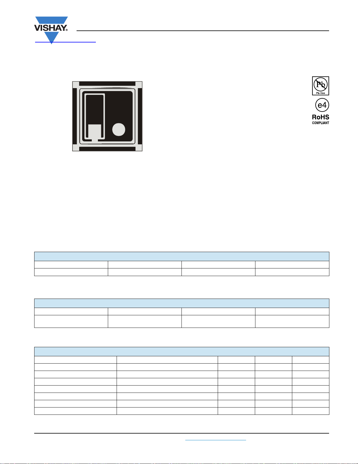
• Package type: chip
• Package form: single chip
• Dimensions (L x W x H in mm): 0.53 x 0.53 x
0.185
• High photo sensitivity
• High radiant sensitivity
• Suitable for visible and near infrared radiation
• Fast response times
21650
DESCRIPTION
T1090P is a silicon NPN phototransistor chip with high
radiant sensitivity, sensitive to visible and near infrared
radiation.
GENERAL INFORMATION
The datasheet is based on Vishay optoelectronics sample testing under certain predetermined and assumed conditions, and is
provided for illustration purpose only. Customers are encouraged to perform testing in actual proposed packaged and used
conditions. Vishay optoelectronics die products are tested using Vishay optoelectronics based quality assurance procedures and
are manufactured using Vishay optoelectronics established processes. Estimates such as those described and set forth in this
datasheet for semiconductor die will vary depending on a number of packaging, handling, use, and other factors. Therefore sold
die may not perform on an equivalent basis to standard package products.
• Compliant to RoHS directive 2002/95/EC and in
accordance to WEEE 2002/96/EC
APPLICATIONS
• Detector in electronic control and drive circuits
PRODUCT SUMMARY
COMPONENT Ica (mA) ϕ (deg) λ
T1090P 0.43 to 0.77 ± 60 440 to 1070
Note
Test condition see table “Basic Characteristics”
0.1
(nm)
ORDERING INFORMATION
ORDERING CODE PACKAGING REMARKS PACKAGE FORM
T1090P-SD-F
Note
MOQ: minimum order quantity
Wafer sawn on foil with disco
frame
MOQ: 50 000 pcs Chip
ABSOLUTE MAXIMUM RATINGS
PARAMETER TEST CONDITION SYMBOL VALUE UNIT
Collector emitter voltage V
Emitter collector voltage V
Collector current I
Junction temperature T
Operating temperature range T
Storage temperature range T
Storage temperature range on foil T
Note
T
= 25 °C, unless otherwise specified
amb
Document Number: 81123 For technical questions, contact: optochipsupport@vishay.com
Rev. 1.4, 29-Mar-10 1
CEO
ECO
C
j
amb
stg1
stg2
70 V
5V
50 mA
100 °C
- 40 to + 100 °C
- 40 to + 100 °C
- 40 to + 50 °C
www.vishay.com
T1090P
Vishay Semiconductors
查询"T1090P"供应商
BASIC CHARACTERISTICS
(1)
Silicon NPN Phototransistor
PARAMETER TEST CONDITION SYMBOL MIN. TYP. MAX. UNIT
Collector emitter breakdown voltage I
Collector emitter dark current V
Collector light current
(Vishay selection type
3
)
= 1 mW/cm2, λ = 950 nm,
E
e
Wavelength of peak sensitivity λ
Range of spectral bandwidth λ
Rise time V
Fall time V
= 5 V, IC = 2 mA, RL = 100 Ω tr, t
CE
= 5 V, IC = 2 mA, RL = 100 Ω tr, t
CE
= 1 mA V
C
= 20 V, E = 0 I
CE
V
= 5 V
CE
(BR)CEO
CEO
I
ca
p
0.1
f
f
70 V
1nA
0.43 0.77 mA
825 nm
440 to 1070 nm
4.3 µs
7.7 µs
Note
(1)
T
= 25 °C, unless otherwise specified
amb
(2)
The measurements are based on samples of die which are mounted on a TO-header without resin coating
(3)
Specific selection types possible
BASIC CHARACTERISTICS
T
= 25 °C, unless otherwise specified
amb
100
90
80
70
60
50
40
30
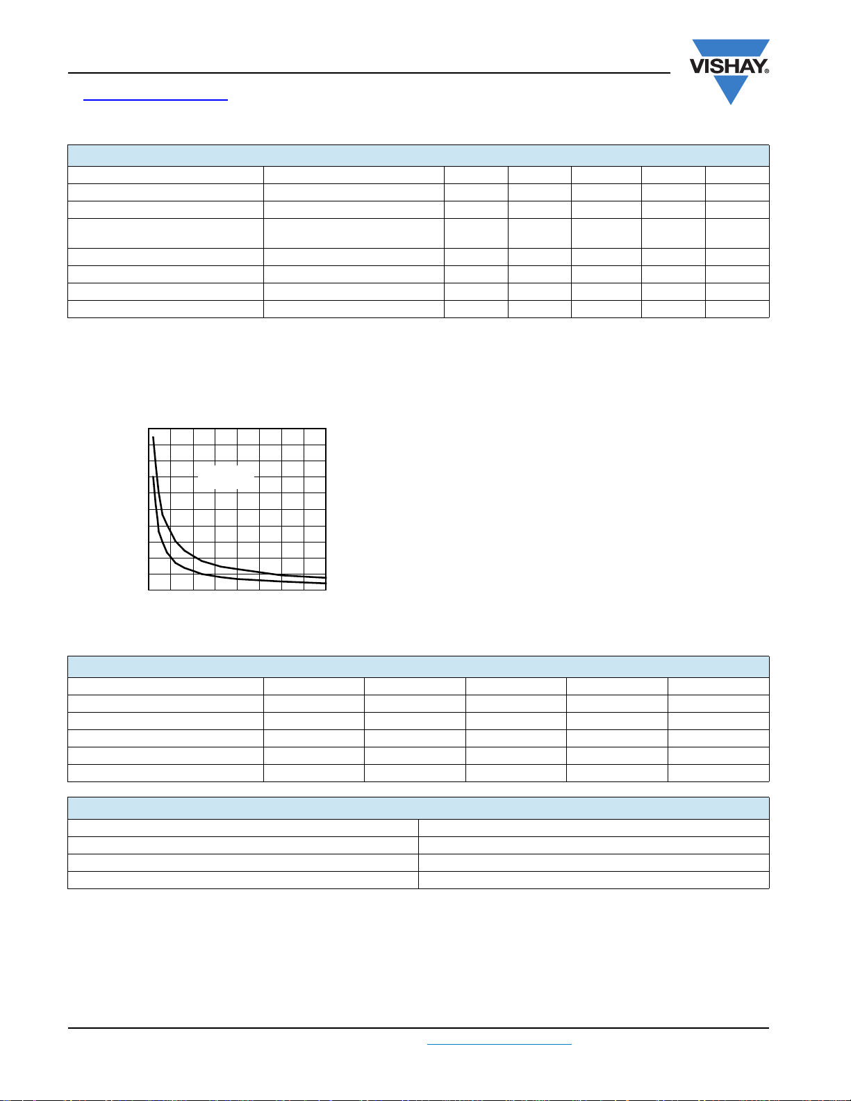
- Rise/Fall Time (µs)
f
t
/t
t
20599
r
r
20
10
0
0 250 500 750 1000 1250 1500 1750 2000
RL = 100 Ω
t
f
- Collector Current (µA)
I
C
Fig. 1 - Rise/Fall Time vs. Collector Current
MECHANICAL DIMENSIONS
PARAMETER SYMBOL MIN. TYP. MAX. UNIT
Length of chip edge (x-direction) L
Length of chip edge (y-direction) L
x
y
Die height H 0.185 mm
Diameter of bond pad base d 0.1 mm
Bond pad emitter a x b 0.1 x 0.1 mm
ADDITIONAL INFORMATION
(1)
Frontside metallization, base (B), emitter (E) Aluminum
Backside metallization, collector AuSb
Dicing Sawing
Die bonding technology Epoxy bonding
Note
(1)
All chips are checked in accordance with the Vishay Semiconductor, specification of visual inspection FVOV6870.
The visual inspection shall be made in accordance with the “specification of visual inspection as referenced”. The visual inspection of chip
backside is performed with stereo microscope with incident light and 40x to 80x magnification.
The quality inspection (final visual inspection) is performed by production. An additional visual inspection step as special release procedure
by QM is not installed.
www.vishay.com For technical questions, contact: optochipsupport@vishay.com
2 Rev. 1.4, 29-Mar-10
0.52 mm
0.52 mm
2
Document Number: 81123

T1090P
查询"T1090P"供应商
Silicon NPN Phototransistor
Vishay Semiconductors
HANDLING AND STORAGE CONDITIONS
• The hermetically sealed shipment lots shall be opened in temperature and moisture controlled cleanroom environment only. It
is mandatory to follow the rules for disposition of material that can be hazardous for humans and environment.
• Product must be handled only at ESD safe workstations. Standard ESD precautions and safe work environments are as defined
in MIL-HDBK-263.
• Singulated die are not to be handled with tweezers. A vacuum wand with non metallic ESD protected tip should be used.
PACKING
Chips are fixed on adhesive foil. Upon request the foils can be mounted on plastic frame or disco frame. For shipment, the wafers
are arranged to stacks and hermetically sealed in plastic bags to ensure protection against environmental influence (humidity and
contamination).
Use for recycling reliable operators only. We can help getting in touch with your nearest sales office. By agreement we will take
back packing material, if it is sorted. You will have to bear the costs of transport. We will invoice you for any costs incurred for
packing material that is returned unsorted or which we are not obliged to accept.
Document Number: 81123 For technical questions, contact: optochipsupport@vishay.com
Rev. 1.4, 29-Mar-10 3
www.vishay.com

Legal Disclaimer Notice
查询"T1090P"供应商
Vishay
Disclaimer
All product specifications and data are subject to change without notice.
Vishay Intertechnology, Inc., its affiliates, agents, and employees, and all persons acting on its or their behalf
(collectively, “Vishay”), disclaim any and all liability for any errors, inaccuracies or incompleteness contained herein
or in any other disclosure relating to any product.
Vishay disclaims any and all liability arising out of the use or application of any product described herein or of any
information provided herein to the maximum extent permitted by law. The product specifications do not expand or
otherwise modify Vishay’s terms and conditions of purchase, including but not limited to the warranty expressed
therein, which apply to these products.
No license, express or implied, by estoppel or otherwise, to any intellectual property rights is granted by this
document or by any conduct of Vishay.
The products shown herein are not designed for use in medical, life-saving, or life-sustaining applications unless
otherwise expressly indicated. Customers using or selling Vishay products not expressly indicated for use in such
applications do so entirely at their own risk and agree to fully indemnify Vishay for any damages arising or resulting
from such use or sale. Please contact authorized Vishay personnel to obtain written terms and conditions regarding
products designed for such applications.
Product names and markings noted herein may be trademarks of their respective owners.
Document Number: 91000 www.vishay.com
Revision: 18-Jul-08 1
 Loading...