

TO-200AC (B-PUK)
PRODUCT SUMMARY
I
T(AV)
ST733CLPbF Series
Vishay High Power Products
Inverter Grade Thyristors
(Hockey PUK Version), 940 A
FEATURES
• Metal case with ceramic insulator
• All diffused design
• Center amplifying gate
• Guaranteed high dV/dt
• Guaranteed high dI/dt
• International standard case TO-200AC (B-PUK)
• High surge current capability
• Low thermal impedance
• High speed performance
• Lead (Pb)-free
• Designed and qualified for industrial level
940 A
TYPICAL APPLICATIONS
•Inverters
• Choppers
• Induction heating
• All types of force-commutated converters
RoHS
COMPLIANT
MAJOR RATINGS AND CHARACTERISTICS
PARAMETER TEST CONDITIONS VALUES UNITS
I
T(AV)
I
T(RMS)
I
TSM
2
I
t
V
DRM/VRRM
t
q
T
J
T
hs
T
hs
50 Hz 20 000
60 Hz 20 950
50 Hz 2000
60 Hz 1820
Range 10 to 20 µs
940 A
55 °C
1900 A
25 °C
400 to 800 V
- 40 to 125 °C
ELECTRICAL SPECIFICATIONS
VOLTAGE RATINGS
TYPE NUMBER
ST733C..L
V
VOLTAGE
CODE
04 400 500
08 800 900
DRM/VRRM
REPETITIVE PEAK VOLTAGE
, MAXIMUM
V
V
, MAXIMUM
NON-REPETITIVE PEAK VOLTAGE
RSM
V
I
DRM/IRRM
AT T
J
A
kA2s
MAXIMUM
= TJ MAXIMUM
mA
75
Document Number: 94378 For technical questions, contact: ind-modules@vishay.com
Revision: 11-Aug-08 1
www.vishay.com
ST733CLPbF Series
Vishay High Power Products
Inverter Grade Thyristors
(Hockey PUK Version), 940 A
CURRENT CARRYING CAPABILITY
I
FREQUENCY UNITS
180° el
TM
180° el
50 Hz 2200 1900 3580 3100 6800 5920
400 Hz 2050 1660 3600 3130 3750 3240
1000 Hz 1370 1070 2900 2450 2120 1780
2500 Hz 500 370 1220 980 960 770
Recovery voltage V
R
Voltage before turn-on V
D
50 50 50
V
DRM
V
Rise of on-state current dI/dt 50 - - A/µs
Heatsink temperature 40 55 40 55 40 55 °C
Equivalent values for RC circuit 10/0.47 10/0.47 10/0.47 Ω/µF
ABSOLUTE MAXIMUM RATINGS
PARAMETER SYMBOL TEST CONDITIONS VALUES UNITS
Maximum average on-state
current at heatsink temperature
Maximum RMS on-state current I
I
T(RMS)
Maximum peak, one half cycle,
non-repetitive surge current
2
Maximum I
Maximum I
t for fusing I2t
2
√t for fusing I2√t t = 0.1 to 10 ms, no voltage reapplied 20 000 kA2√s
Maximum peak on-state voltage V
Low level value of threshold voltage V
High level value of threshold voltage V
Low level value of forward slope resistance r
High level value of forward slope resistance r
Maximum holding current I
Typical latching current I
T(AV)
I
TSM
TM
T(TO)1
T(TO)2
t1
t2
H
L
180° conduction, half sine wave
double side (single side) cooled
DC at 25 °C heatsink temperature double side cooled 1900
t = 10 ms
t = 8.3 ms 20 950
t = 10 ms
t = 8.3 ms 17 600
t = 10 ms
t = 8.3 ms 1820
t = 10 ms
t = 8.3 ms 1290
No voltage
reapplied
100 % V
reapplied
No voltage
reapplied
100 % V
reapplied
ITM = 1700 A, TJ = TJ maximum,
= 10 ms sine wave pulse
t
p
(16.7 % x π x I
(I > π x I
T(AV)
(16.7 % x π x I
(I > π x I
T(AV)
< I < π x I
T(AV)
), TJ = TJ maximum 1.20
< I < π x I
T(AV)
), TJ = TJ maximum 0.29
TJ = 25 °C, IT > 30 A 600
TJ = 25 °C, VA = 12 V, Ra = 6 Ω, IG = 1 A 1000
DRM
I
TM
RRM
Sinusoidal half wave,
initial T
RRM
), TJ = TJ maximum 1.09
T(AV)
), TJ = TJ maximum 0.32
T(AV)
100 µs
V
= TJ maximum
J
DRM
I
TM
940 (350) A
55 (85) °C
20 000
16 800
2000
1410
1.63
A
V
kA
mΩ
mA
A
2
s
V
www.vishay.com For technical questions, contact: ind-modules@vishay.com
Document Number: 94378
2 Revision: 11-Aug-08
ST733CLPbF Series
Inverter Grade Thyristors
Vishay High Power Products
(Hockey PUK Version), 940 A
SWITCHING
PARAMETER SYMBOL TEST CONDITIONS VALUES UNITS
Maximum non-repetitive rate of
rise of turned-on current
Typical delay time t
dI/dt
d
minimum
Maximum turn-off time
maximum 20
t
q
BLOCKING
PARAMETER SYMBOL TEST CONDITIONS VALUES UNITS
Maximum critical rate of rise of off-state voltage dV/dt
Maximum peak reverse and off-state leakage current
TRIGGERING
PARAMETER SYMBOL TEST CONDITIONS VALUES UNITS
Maximum peak gate power P
Maximum average gate power P
Maximum peak positive gate current I
Maximum peak positive gate voltage + V
Maximum peak negative gate voltage - V
Maximum DC gate current required to trigger I
Maximum DC gate voltage required to trigger V
Maximum DC gate current not to trigger I
Maximum DC gate voltage not to trigger V
= TJ maximum, V
T
J
= Rated V
DRM
, ITM = 2 x dI/dt
DRM
Gate pulse: 20 V 20 Ω, 10 µs 0.5 µs rise time
TJ = 25 °C, VDM = Rated V
, ITM = 50 A DC, tp = 1 µs
DRM
Resistive load, gate pulse: 10 V, 5 Ω source
TJ = TJ maximum,
I
= 550 A, commutating dI/dt = 40 A/µs
TM
V
= 50 V, tp = 500 µs, dV/dt: see table in device code
R
= TJ maximum, linear to 80 % V
T
J
higher value available on request
I
,
RRM
I
DRM
G(AV)
GM
GT
GD
GM
GM
GM
GT
GD
TJ = TJ maximum, rated V
DRM/VRRM
TJ = TJ maximum, f = 50 Hz, d% = 50
TJ = TJ maximum, tp ≤ 5 ms
TJ = 25 °C, VA = 12 V, Ra = 6 Ω
TJ = TJ maximum, rated V
DRM
applied
1000 A/µs
1.5
10
,
DRM
500 V/µs
applied 75 mA
60
10
10 A
20
5
200 mA
3V
20 mA
0.25 V
µs
W
V
THERMAL AND MECHANICAL SPECIFICATIONS
PARAMETER SYMBOL TEST CONDITIONS VALUES UNITS
Maximum operating junction temperature range T
Maximum storage temperature range T
Maximum thermal resistance, junction to heatsink R
Maximum thermal resistance, case to heatsink R
J
Stg
thJ-hs
thC-hs
DC operation single side cooled 0.073
DC operation double side cooled 0.031
DC operation single side cooled 0.011
DC operation double side cooled 0.005
Mounting force, ± 10 %
Approximate weight 255 g
Case style See dimensions - link at the end of datasheet TO-200AC (B-PUK)
Document Number: 94378 For technical questions, contact: ind-modules@vishay.com
Revision: 11-Aug-08 3
- 40 to 125
- 40 to 150
14 700
(1500)
°C
K/W
N
(kg)
www.vishay.com

ST733CLPbF Series
Vishay High Power Products
Inverter Grade Thyristors
(Hockey PUK Version), 940 A
ΔR
Note
• The table above shows the increment of thermal resistance R
CONDUCTION
thJ-hs
CONDUCTION ANGLE
180° 0.009 0.009 0.006 0.006
120° 0.011 0.011 0.011 0.011
90° 0.014 0.014 0.015 0.015
60° 0.020 0.021 0.021 0.022
30° 0.036 0.036 0.036 0.036
130
120
110
100
90
80
70
60
50
40
0 100200300400500600700
Maximum Allowable Heatsink Temperature (°C)
Average On-state Current (A)
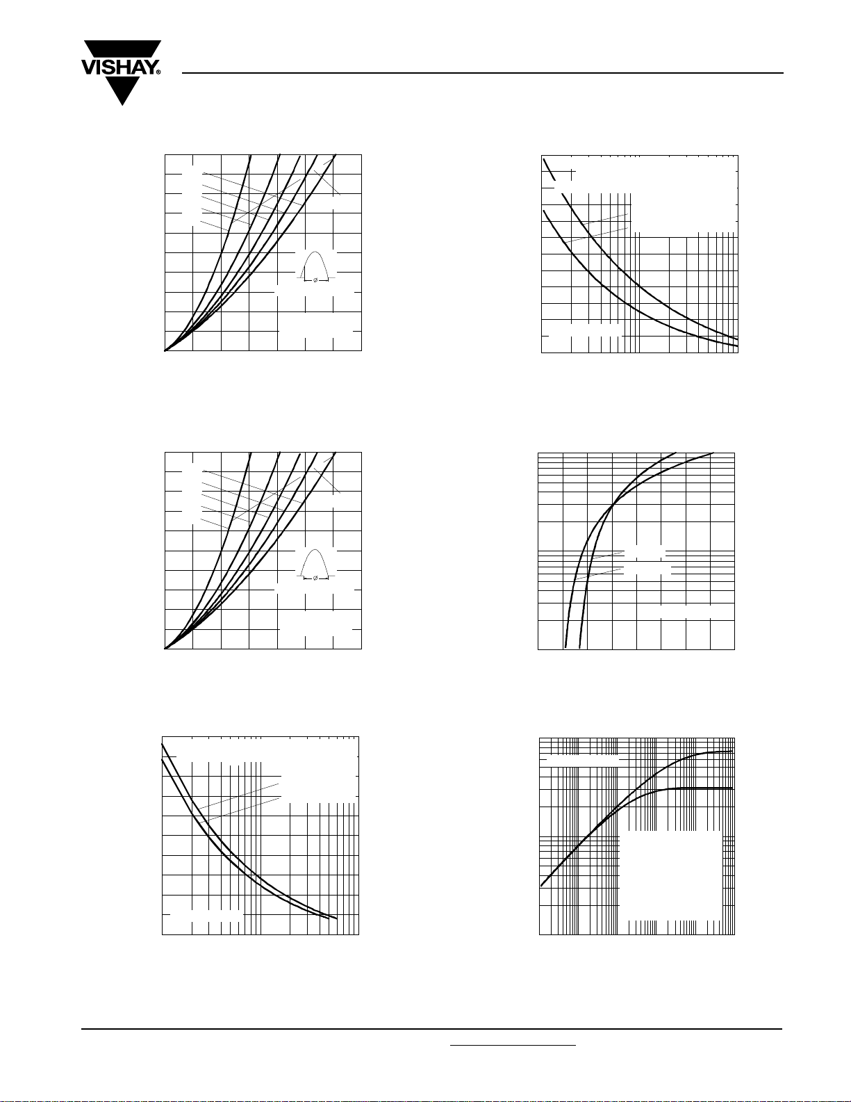
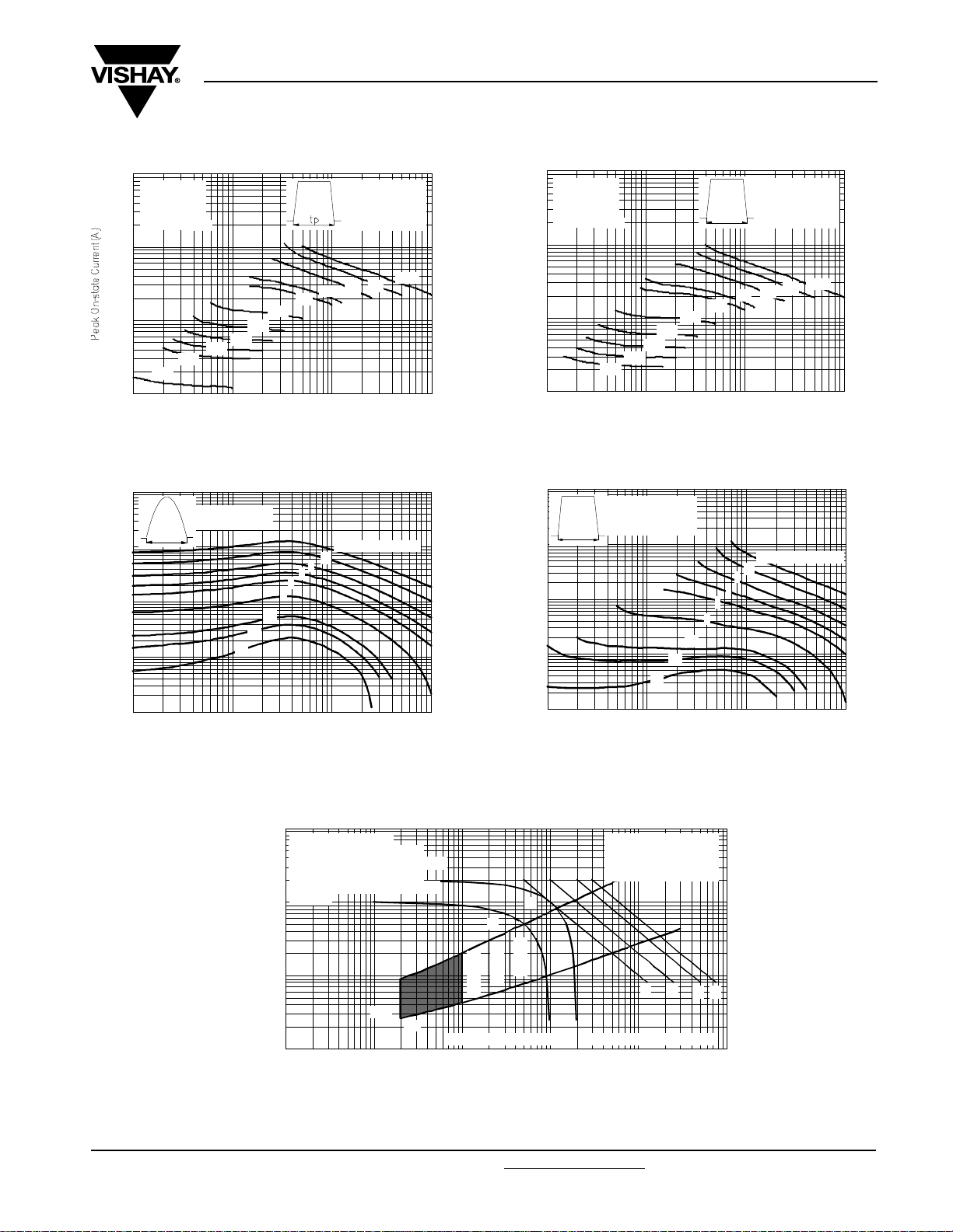
Fig. 1 - Current Ratings Characteristics
SINUSOIDAL CONDUCTION RECTANGULAR CONDUCTION
SINGLE SIDE DOUBLE SIDE SINGLE SIDE DOUBLE SIDE
ST733C..L Se ries
(Single Side Cooled)
R (DC) = 0.073 K/ W
thJ-hs
Cond uction Angle
30°
60°
90°
120°
180°
TEST CONDITIONS UNITS
= TJ maximum K/W
T
J
when devices operate at different conduction angles than DC
thJ-hs
130
120
110
100
90
80
70
60
50
40
30
20
0 200 400 600 800 1000 1200 1400
Maximum Allowable Heatsink Temperature (°C)
Average On-state Current (A)
ST7 33 C . .L Se r i e s
(Double Side Cooled)
R (DC) = 0.031 K/ W
thJ-hs
Cond uctio n Angle
30°
60°
90°
120°
Fig. 3 - Current Ratings Characteristics
180°
130
120
110
100
90
80
70
60
50
40
30
20
0 200 400 600 800 1000
Maximum Allowable He atsink Temperature (°C)
ST7 33 C . . L Se r i e s
(Single Side Cooled)
R (DC) = 0.073 K/W
thJ-hs
Conduction Pe riod
30°
60°
90°
120°
180°
Avera ge On-state Current (A)
Fig. 2 - Current Ratings Characteristics
DC
130
120
110
100
90
80
70
60
50
40
30
20
0 500 1000 1500 2000
Maximum Allowable Heatsink Temperature (°C)
Avera ge On-state Current (A)
ST7 3 3 C . . L Se r i e s
(Double Side Cooled)
R (DC) = 0.031 K/ W
thJ-hs
30°
60°
90°
120°
Conduction Period
180°
Fig. 4 - Current Ratings Characteristics
DC
www.vishay.com For technical questions, contact: ind-modules@vishay.com
Document Number: 94378
4 Revision: 11-Aug-08
ST733CLPbF Series
2500
180°
2000
1500
1000
Maximum Average On-stat e Power Loss (W)
120°
90°
60°
30°
Cond uction Angle
500
0
0 200 400 600 800 1000 1200 1400
Average On-state Current (A)
ST7 3 3 C . . L Se r i e s
T = 125°C
J
Fig. 5 - On-State Power Loss Characteristics
2500
180°
2000
1500
1000
Maximum Average On-state Power Loss (W)
120°
90°
60°
30°
Cond uction Angle
500
0
0 200 400 600 800 1000 1200 1400
Average On-state Current (A)
ST7 33 C . . L Se r i e s
T = 1 2 5° C
J
Fig. 6 - On-State Power Loss Characteristics
Inverter Grade Thyristors
(Hockey PUK Version), 940 A
20000
18000
RM S Li m i t
16000
14000
12000
ine Wav e On -sta te Current ( A)
10000
Pea k Ha lf S
8000
Fig. 8 - Maximum Non-Repetitive Surge Current
10000
RM S Li m i t
1000
Instantaneous On-state Current (A)
100
Fig. 9 - On-State Voltage Drop Characteristics
Vishay High Power Products
Maximum Non Repetitive Surge Current
Versus Pulse Train Duration. Control
Of Conduction May Not Be Maintained.
ST733C..L Se ries
0.01 0.1 1
Pulse Train Duration (s)
Single and Double Side Cooled
0.5 1 1.5 2 2.5 3 3.5 4 4.5
Instantaneous On-state Voltage (V)
Init ia l T = 125°C
No Vo lta ge Re a p plied
Ra t e d V Re a p p l ie d
T = 2 5 ° C
J
T = 125°C
J
ST733C..L Serie s
J
RRM
18000
16000
14000
12000
10000
Peak Half Sine Wave On -sta te C urrent (A)
8000
Numb er O f Eq ual Amp lit ude Half C ycl e C urrent Pulses (N)
At Any Rat e d Loa d Co ndition A n d Wit h
Rated V Applied Following Surge.
RRM
ST733C..L Series
110100
Init ial T = 125° C
J
@ 60 Hz 0.0083 s
@ 50 Hz 0.0100 s
Fig. 7 - Maximum Non-Repetitive Surge Current
Single and Double Side Cooled
0.1
ST7 3 3C . .L Se r ie s
thJ-hs
0.01
0.001
Transient Thermal Impedance Z (K/W)
0.001 0.01 0.1 1 10 100
Square Wave Pulse Duration (s)
Fig. 10 - Thermal Impedance Z
St e a d y St a t e V a lu e
R = 0.073 K/W
thJ-hs
(Single Side Co oled )
R = 0.031 K/W
thJ-hs
(Double Side Cooled)
(DC Operat ion)
thJC
Characteristics
Document Number: 94378 For technical questions, contact: ind-modules@vishay.com
www.vishay.com
Revision: 11-Aug-08 5

ST733CLPbF Series
Vishay High Power Products
450
1000
I = 1500 A
TM
1000 A
500 A
200
400
tp
ST7 33 C . . L Se r i e s
400
T = 125 °C
J
350
300
250
200
150
100
50
0
10 20 30 40 50 60 70 80 90 100
Ma xim um Rev e rse Rec ove ry C harg e - Qrr (µC)
Rate Of Fall Of On-state Current - di/dt (A/µs)
Fig. 11 - Reverse Recovered Charge Characteristics Fig. 12 - Reverse Recovered Current Characteristics
1E5
1E4
1500
1E3
Peak On-state Current (A)
1E2
1E11E21E31E4
2500
3000
5000
Pul se Ba se w id th (µ s)
Inverter Grade Thyristors
(Hockey PUK Version), 940 A
250
200
150
100
50
0
Maximum Reverse Recovery Current - Irr (A)
Rate Of Fall Of Forward Current - di/dt (A/µs)
Sn u b b e r c i r c u i t
R = 10 o hm s
s
C = 0.47 µF
s
V = 80% V
D
100
ST733C.. L Serie s
Sinusoid al p ulse
T = 40°C
C
50 Hz
DRM
1E1 1E2 1E3 1E4
1E1
I = 1500 A
TM
1000 A
500 A
ST733C..L Se ries
T = 125 °C
J
10 20 30 40 50 60 70 80 90 100
Snu bb er c irc ui t
R = 10 o h ms
s
C = 0.47 µF
s
V = 80% V
D
100
200
400
1000
1500
2500
tp
ST7 33 C . . L Series
Si n u so i d a l p u l s e
T = 55 ° C
C
3000
5000
Pu l se Ba sew id t h ( µs)
DRM
50 Hz
Fig. 13 - Frequency Characteristics
1E5
Snubbe r circuit
R = 10 ohms
s
C = 0.47 µF
s
V = 80% V
D
DRM
1E4
1000
1E3
5000
1E2
1E1 1E2 1E3 1E4
1500
2000
2500
3000
Pulse Basewidth (µs)
500
400
ST733C..L Series
Trapezoidal pulse
T = 40°C
C
di/ dt = 50A/ µs
100
200
50 Hz
Snubber circuit
R = 10 ohms
s
C = 0.47 µF
s
V = 80% V
D
DRM
1000
1500
2000
2500
3000
1E1 1E2 1E3 1E4
Pulse Basewidth (µs)
tp
500
ST733C..L Series
Trapezoidal pulse
T = 55°C
C
di/ dt = 50A/µs
100
200
400
50 Hz
Fig. 14 - Frequency Characteristics
www.vishay.com For technical questions, contact: ind-modules@vishay.com
Document Number: 94378
6 Revision: 11-Aug-08
ST733CLPbF Series
Inverter Grade Thyristors
(Hockey PUK Version), 940 A
1E5
Snubbe r circuit
R = 10 ohms
s
C = 0.47 µF
s
V = 80% V
D
DRM
1E4
1E3
2500
3000
5000
1E2
1E1 1E2 1E3 1E4
1000
1500
2000
Pulse Basewidth (µs)
1E5
ST733C.. L Se rie s
Sinusoid al p ulse
tp
1E4
2
1E3
1E2
Peak On-state Current (A)
1
0.5
0.4
0.3
500
400
10
5
3
ST733C..L Series
Trapezoidal pulse
T = 40°C
C
di/ dt = 100A/µs
100
200
20 jou le s per p ulse
Snubber circuit
R = 10 ohms
s
C = 0.47 µF
s
V = 80% V
D
50 Hz
1E1 1E2 1E3 1E4
Fig. 15 - Frequency Characteristics
tp
Vishay High Power Products
ST733C..L Series
Trapezoidal pulse
T = 55°C
C
tp
500
2
di/ dt = 100A/ µs
200
400
20 jou le s p er pu lse
10
5
3
100
50 Hz
DRM
1500
2000
2500
3000
Pulse Basewidth (µs)
ST7 33 C . . L Se r i e s
Re c t a n gu l a r p u l se
di/dt = 50A/µs
0.4
0.3
1000
1
0.5
1E1
1E1 1E2 1E3 1E4
Pu l se Ba se w id t h ( µs)
1E1 1E2 1E3 1E4
Pu l se Ba sew id t h (µ s)
Fig. 16 - Maximum On-State Energy Power Loss Characteristics
100
Rectangular gate pulse
a) Reco mmend ed l oa d l ine for
rated d i/ dt : 20V, 10ohms; tr<=1 µs
b) Reco mmend ed l oa d l ine for
<=30% rate d di/ dt : 10V, 10ohms
tr<=1 µs
10
Tj=125 °C
1
Instantane ous Gate Voltage (V)
0.1
0.001 0. 01 0.1 1 10 100
VGD
IGD
Dev ice: ST733C..L Serie s
Instantaneous Gate Current (A)
(b)
Tj=25 °C
(a)
Tj=40 °C
(1) PGM = 10W, tp = 20ms
(2) PGM = 20W, tp = 10ms
(3) PGM = 40W, tp = 5ms
(4) PGM = 60W, tp = 3.3ms
(1) (2) (3)
Frequency Limited by PG(AV)
(4)
Fig. 17 - Gate Characteristics
Document Number: 94378 For technical questions, contact: ind-modules@vishay.com
www.vishay.com
Revision: 11-Aug-08 7
ST733CLPbF Series
Vishay High Power Products
ORDERING INFORMATION TABLE
Device code
ST 73 3 C 08 L H K 1 - P
324
1 - Thyristor
2 - Essential part number
3 - 3 = Fast turn-off
4 - C = Ceramic PUK
5 - Voltage code x 100 = V
(see Voltage Ratings table)
6 - L = PUK case TO-200AC (B-PUK)
7 - Reapplied dV/dt code (for t
8 -t
9 - 0 = Eyelet terminals
10
11
code
q
(gate and auxiliary cathode unsoldered leads)
1 = Fast-on terminals
(gate and auxiliary cathode unsoldered leads)
2 = Eyelet terminals
(gate and auxiliary cathode soldered leads)
3 = Fast-on terminals
(gate and auxiliary cathode soldered leads)
- Critical dV/dt:
None = 500 V/µs (standard value)
L = 1000 V/µs (special selection)
- P = Lead (Pb)-free
Inverter Grade Thyristors
(Hockey PUK Version), 940 A
51
6 7 8 9 10 11
RRM
dV/dt - tq combinations available
test condition)
q
t
q
* Standard part number.
All other types available only on request.
dV/dt (V/µs) 20 50 100 200 400
(µs)
10
12
15
18
20
CN DN EN
CM DM EM
CL DL EL
CP DP EP FP HP
CK DK EK FK H
FM*
FL*
--
-
HL
LINKS TO RELATED DOCUMENTS
Dimensions http://www.vishay.com/doc?95076
www.vishay.com For technical questions, contact: ind-modules@vishay.com
8 Revision: 11-Aug-08
Document Number: 94378

DIMENSIONS in millimeters (inches)
Pin receptacle
AMP. 60598-1
0.7 (0.03) MIN.
34 (1.34) DIA. MAX.
2 places
53 (2.09) DIA. MAX.
58.5 (2.3) DIA. MAX.
2 holes DIA. 3.5 (0.14) x 2.5 (0.1) deep
4.7 (0.18)
27 (1.06) MAX.
0.7 (0.03) MIN.
6.2 (0.24) MIN.
36.5 (1.44)
Creepage distance: 36.33 (1.430) minimum
Strike distance: 17.43 (0.686) minimum
Quote between upper and lower pole pieces has to be considered after
application of mounting force (see thermal and mechanical specification)
20° ± 5°
Outline Dimensions
Vishay Semiconductors
TO-200AC (B-PUK)
Document Number: 95076 For technical questions, contact: indmodules@vishay.com
Revision: 01-Aug-07 1
www.vishay.com

Legal Disclaimer Notice
www.vishay.com
Vishay
Disclaimer
ALL PRODUCT, PRODUCT SPECIFICATIONS AND DATA ARE SUBJECT TO CHANGE WITHOUT NOTICE TO IMPROVE
RELIABILITY, FUNCTION OR DESIGN OR OTHERWISE.
Vishay Intertechnology, Inc., its affiliates, agents, and employees, and all persons acting on its or their behalf (collectively,
“Vishay”), disclaim any and all liability for any errors, inaccuracies or incompleteness contained in any datasheet or in any other
disclosure relating to any product.
Vishay makes no warranty, representation or guarantee regarding the suitability of the products for any particular purpose or
the continuing production of any product. To the maximum extent permitted by applicable law, Vishay disclaims (i) any and all
liability arising out of the application or use of any product, (ii) any and all liability, including without limitation special,
consequential or incidental damages, and (iii) any and all implied warranties, including warranties of fitness for particular
purpose, non-infringement and merchantability.
Statements regarding the suitability of products for certain types of applications are based on Vishay’s knowledge of typical
requirements that are often placed on Vishay products in generic applications. Such statements are not binding statements
about the suitability of products for a particular application. It is the customer’s responsibility to validate that a particular
product with the properties described in the product specification is suitable for use in a particular application. Parameters
provided in datasheets and/or specifications may vary in different applications and performance may vary over time. All
operating parameters, including typical parameters, must be validated for each customer application by the customer’s
technical experts. Product specifications do not expand or otherwise modify Vishay’s terms and conditions of purchase,
including but not limited to the warranty expressed therein.
Except as expressly indicated in writing, Vishay products are not designed for use in medical, life-saving, or life-sustaining
applications or for any other application in which the failure of the Vishay product could result in personal injury or death.
Customers using or selling Vishay products not expressly indicated for use in such applications do so at their own risk. Please
contact authorized Vishay personnel to obtain written terms and conditions regarding products designed for such applications.
No license, express or implied, by estoppel or otherwise, to any intellectual property rights is granted by this document or by
any conduct of Vishay. Product names and markings noted herein may be trademarks of their respective owners.
Material Category Policy
Vishay Intertechnology, Inc. hereby certifies that all its products that are identified as RoHS-Compliant fulfill the
definitions and restrictions defined under Directive 2011/65/EU of The European Parliament and of the Council
of June 8, 2011 on the restriction of the use of certain hazardous substances in electrical and electronic equipment
(EEE) - recast, unless otherwise specified as non-compliant.
Please note that some Vishay documentation may still make reference to RoHS Directive 2002/95/EC. We confirm that
all the products identified as being compliant to Directive 2002/95/EC conform to Directive 2011/65/EU.
Vishay Intertechnology, Inc. hereby certifies that all its products that are identified as Halogen-Free follow Halogen-Free
requirements as per JEDEC JS709A standards. Please note that some Vishay documentation may still make reference
to the IEC 61249-2-21 definition. We confirm that all the products identified as being compliant to IEC 61249-2-21
conform to JEDEC JS709A standards.
Revision: 02-Oct-12
1
Document Number: 91000
 Loading...