

Bulletin I25187 rev. B 04/00
ST333C..L SERIES
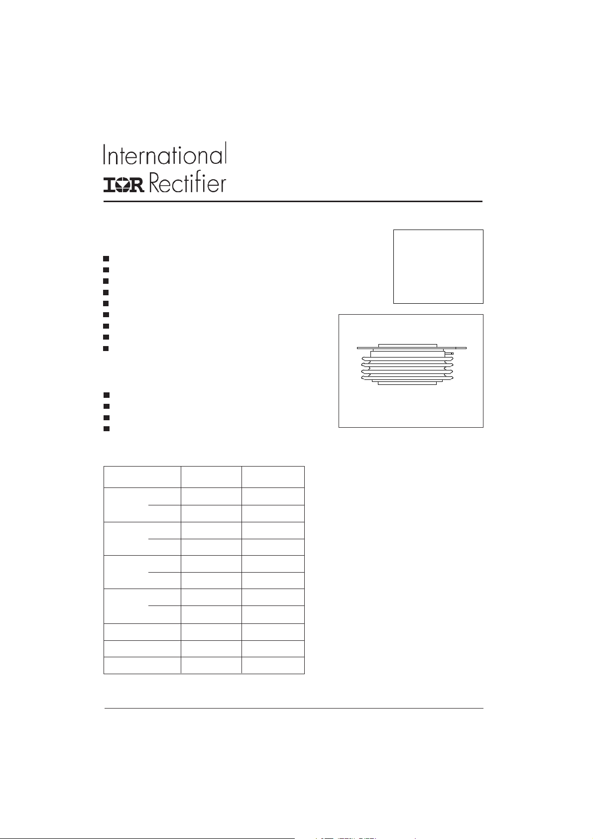
INVERTER GRADE THYRISTORS Hockey Puk Version
Features
Metal case with ceramic insulator
International standard case TO-200AC (B-PUK)
All diffused design
Center amplifying gate
Guaranteed high dV/dt
Guaranteed high dI/dt
High surge current capability
Low thermal impedance
High speed performance
Typical Applications
Inverters
Choppers
Induction heating
All types of force-commutated converters
case style TO-200AC (B-PUK)
620A
Major Ratings and Characteristics
Parameters ST333C..L Units
I
T(AV)
@ T
hs
I
T(RMS)
@ T
hs
I
TSM
I2t@
V
DRM/VRRM
tq range 10 to 30 µs
T
J
@ 50Hz 11000 A
@ 60Hz 11500 A
50Hz 605 KA2s
@ 60Hz 553 KA
www.irf.com
620 A
55 °C
1230 A
25 °C
400 to 800 V
- 40 to 125 °C
2
s
1
ST333C..L Series
Bulletin I25187 rev. B 04/00
ELECTRICAL SPECIFICATIONS
Voltage Ratings
Voltage V
DRM/VRRM
Type number Code repetitive peak voltage non-repetitive peak voltage @ T
ST333C..L 50
04 400 500
08 800 900
Current Carrying Capability
, maximum V
, maximum I
RSM
DRM/IRRM
VVmA
max.
= TJ max.
J
I
Frequency Units
180
TM
o
el
180oel
I
TM
100µs
I
TM
50Hz 1430 1250 2340 1940 6310 5620
400Hz 1670 1170 2310 2010 3440 5030
1000Hz 1080 880 2090 1800 2040 1750
2500Hz 530 400 1190 990 990 800
Recovery voltage Vr 50 50 50 50 50 50
Voltage before turn-on Vd V
DRM
V
DRM
V
DRM
Rise of on-state current di/dt 50 50 - - - - A/µs
Heatsink temperature 40 55 40 55 40 55 °C
Equivalent values for RC circuit 10Ω / 0.47µF 10Ω / 0.47µF 10Ω / 0.47µF
On-state Conduction
Parameter ST333C..L Units Conditions
I
Max. average on-state current 620 (305) A 180° conduction, half sine wave
T(AV)
@ Heatsink temperature 55 (75) °C double side (single side) cooled
I
Max. RMS on-state current 1230 DC @ 25°C heatsink temperature double side cooled
T(RMS)
I
Max. peak, one half cycle, 11000 t = 10ms No voltage
TSM
non-repetitive surge current 11500 A t = 8.3ms reapplied
9250 t = 10ms 100% V
9700 t = 8.3ms reapplied Sinusoidal half wave,
2
t Maximum I2t for fusing 605 t = 10ms No voltage Initial TJ = TJ max
I
553 t = 8.3ms reapplied
428 t = 10ms 100% V
KA2s
391 t = 8.3ms reapplied
2
I
√t Maximum I2√t for fusing 6050 KA2√s t = 0.1 to 10ms, no voltage reapplied
RRM
RRM
A
V
2
www.irf.com
ST333C..L Series
Bulletin I25187 rev. B 04/00
On-state Conduction
Parameter ST333C..L Units Conditions
VTMMax. peak on-state voltage 1.96 ITM= 1810A, TJ = TJ max, tp = 10ms sine wave pulse
Low level value of threshold
V
T(TO)1
voltage
High level value of threshold
V
T(TO)2
voltage
Low level value of forward
r
1
t
slope resistance
High level value of forward
r
t2
slope resistance
Maximum holding current 600 TJ = 25°C, IT > 30A
I
H
Typical latching current 1000 TJ = 25°C, VA= 12V, Ra = 6Ω, IG= 1A
I
L
Switching
Parameter ST333C..L Units Conditions
di/dt Max. non-repetitive rate of rise T
of turned-on current I
t
Typical delay time 1.1
d
t
Max. turn-off time
q
0.91 (16.7% x π x I
V
0.93 (I > π x I
0.58 (16.7% x π x I
mΩ
0.58 (I > π x I
mA
= TJ max, V
1000 A/µs
Min Max
10 30
J
= 2 x di/dt
TM
= 25°C, V
T
J
Resistive load, Gate pulse: 10V, 5Ω source
µs
= TJ max, I
T
J
= 50V, tp = 500µs, dv/dt: see table in device code
V
R
< I < π x I
T(AV)
), TJ = TJ max.
T(AV)
< I < π x I
T(AV)
), TJ = TJ max.
T(AV)
DRM
= rated V
DM
= 550A, commutating di/dt = 40A/µs
TM
= rated V
DRM, ITM
T(AV)
T(AV)
DRM
= 50A DC, tp= 1µs
), TJ = TJ max.
), TJ = TJ max.
Blocking
Parameter ST333C..L Units Conditions
dv/dt Maximum critical rate of rise of T
off-state voltage available on request
Max. peak reverse and off-state
I
RRM
leakage current
I
DRM
500 V/µs
50 mA T
Triggering
Parameter ST333C..L Units Conditions
PGMMaximum peak gate power 60
Maximum average gate power 10
P
G(AV)
I
Max. peak positive gate current 10 A TJ = TJ max, tp ≤ 5ms
GM
+VGMMaximum peak positive
gate voltage
Maximum peak negative
-V
GM
gate voltage
Max. DC gate current required
I
GT
to trigger
V
Max. DC gate voltage required
GT
to trigger
Max. DC gate current not to trigger 20 mA
I
GD
V
Max. DC gate voltage not to trigger 0.25 V
GD
20
5
200 mA
3V
WTJ = TJ max., f = 50Hz, d% = 50
VTJ = TJ max, tp ≤ 5ms
T
TJ = TJ max, rated V
www.irf.com
= TJ max. linear to 80% V
J
= TJ max, rated V
J
= 25°C, VA = 12V, Ra = 6Ω
J
DRM/VRRM
applied
DRM
, higher value
DRM
applied
3

ST333C..L Series
Bulletin I25187 rev. B 04/00
Thermal and Mechanical Specification
Parameter ST333C..L Units Conditions
TJMax. operating temperature range -40 to 1 25
Max. storage temperature range -40 t o 1 50
T
stg
R
Max. thermal resistance, 0.11 DC operation single side cooled
thJ-hs
junction to heatsink 0.05 DC operation double side cooled
R
Max. thermal resistance, 0.011 DC operation single side cooled
thC-hs
case to heatsink 0.005 DC operation double side cooled
F Mounting force, ± 10% 9800 N
(1000) (Kg)
wt Approximate weight 250 g
Case style TO - 200AC (B-PUK) See Outline Table
∆R
Conduction
thJ-hs
(The following table shows the increment of thermal resistence R
Conduction angle Units Conditions
180° 0.012 0.010 0.008 0.008
120° 0.014 0.015 0.014 0.014
90° 0.018 0.018 0.019 0.019 K/W T
60° 0.026 0.027 0.027 0.028
30° 0.045 0.046 0.046 0.046
Sinusoidal conduction Rectangular conduction
Single Side Double Side Single Side Double Side
Ordering Information Table
°C
K/W
K/W
when devices operate at different conduction angles than DC)
thJ-hs
J
= TJ max.
Device Code
ST 33 3 C 08 L H K 1
12
1 - Thyristor
2 - Essential part number
3 - 3 = Fast turn off
4 - C = Ceramic Puk
5 - Voltage code: Code x 100 = V
RRM
6 - L = Puk Case TO-200AC (B-PUK)
7 - Reapplied dv/dt code (for tq test condition)
8 -tq code
9 - 0 = Eyelet term. (Gate and Aux. Cathode Unsoldered Leads)
1 = Fast-on term. (Gate and Aux. Cathode Unsoldered Leads)
2 = Eyelet term. (Gate and Aux. Cathode Soldered Leads)
3 = Fast-on term. (Gate and Aux. Cathode Soldered Leads)
- Critical dv/dt:
10
None = 500V/µsec (Standard value)
L = 1000V/µsec (Special selection)
34
(See Voltage Rating Table)
4
6
5
7
9
8
dv/dt - tq combinations available
dv/dt (V/µs) 20 50 100 200 400
10 CN DN EN - - -12 CM DM EM FM * -15 CL DL EL FL * HL
tq(µs)
18 CP DP EP FP HP
20 CK DK EK FK HK
25 -- -- -- FJ HJ
30 -- -- -- -- HH
*Standard part number.
All other types available only on request.
10
www.irf.com

Outline Table
ST333C..L Series
Bulletin I25187 rev. B 04/00
0.7 (0.03) MIN.
27 (1.06) MAX.
0.7 (0.03) MIN.
34 (1.34) DIA. MAX.
TWO PLACES
53 (2.09) DIA. MAX.
5 8 .5 (2 .3 ) D IA . M A X .
2 HOLES DIA. 3.5 (0.14) x
2.5 (0.1) DEEP
CREPAGE DISTANCE 36.33 (1.430) MIN.
STRIKE DISTANCE 17.43 (0.686) MIN.
6.2 (0.24) MIN.
36.5 (1.44)
PIN RECEPTACLE
AMP. 60598-1
4.7 (0.18)
20°± 5°
Case Style TO-200AC (B-PUK)
All dimensions in millimeters (inches)
Quote between upper and lower
pole pieces has to be considered
after application of Mounting Force
(see Thermal and Mechanical
Specification)
130
120
110
ST333C..L Serie s
(Single Side Cooled )
R (DC) = 0.11 K/W
th J-hs
100
90
80
70
60
30°
60°
90°
50
40
30
0 100 200 300 400 500
Maximum Allowable Heatsink Tem perature (°C)
Average On-state Current (A)
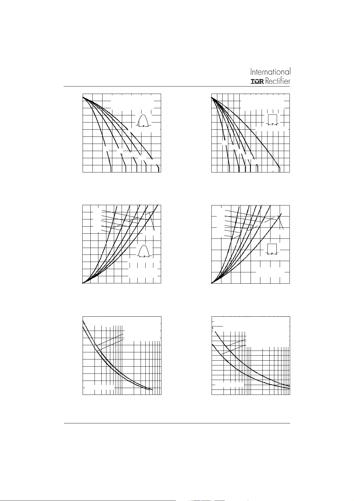
Fig. 1 - Current Ratings Characteristics Fig. 2 - Current Ratings Characteristics
www.irf.com
Con duc tion Angle
120°
180°
130
120
110
ST3 33C ..L Se rie s
(Single S ide Co oled)
R (DC ) = 0.11 K/W
thJ-h s
100
90
80
70
Cond uc tion Period
60
50
30°
60°
90°
120°
180°
40
30
20
0 100 200 300 400 500 600 700 800
M aximum Allowa ble Heatsin k Temperature (°C)
A ve ra g e O n -sta te C urre n t (A )
DC
5
ST333C..L Series
Bulletin I25187 rev. B 04/00
130
120
110
ST333C ..L Series
(Double Side Cooled)
R (DC ) = 0.05 K /W
thJ- hs
100
90
80
Cond uction A ngle
70
60
50
40
30°
60°
90°
30
20
0 100 200 300 400 500 600 700 800
Maximum Allow able Heatsink Temperature (°C)
Average On-state Current (A)
Fig. 3 - Current Ratings Characteristics Fig. 4 - Current Ratings Characteristics
2200
2000
1800
1600
1400
180°
120°
90°
60°
30°
1200
1000
800
600
400
200
0
Maximum Average On -state Power Loss (W)
0 200 400 600 800 1000
Con duc tion Angle
ST333C..L Series
T = 125°C
J
Average On-state Current (A)
Fig. 5 - On-state Power Loss Characteristics
120°
RMS Limit
180°
130
120
110
ST333C ..L Series
(Double Side Co oled)
R (D C) = 0.05 K/W
th J-hs
100
90
80
Conduction Period
70
30°
60
50
40
30
20
0 200 400 600 800 1000 1200 1400
Maxim um Allowable Heatsink Temperature (° C)
60°
90°
120°
180°
Averag e O n-state C urrent (A)
2800
DC
180°
2400
120°
2000
1600
90°
60°
30°
1200
800
400
0
Maximum Average On-state Power Loss (W)
0 200 400 600 800 1000 1200 1400 1600
Conduction Period
ST333C ..L Series
T = 125°C
J
Average On-state Current (A)
Fig. 6 - On-state Power Loss Characteristics
DC
RMS Limit
10000
At An y Ra ted Loa d Co ndition And W i th
9500
Rated V Applied Following Surge.
9000
RRM
8500
Init ial T = 125°C
J
@ 60 Hz 0.0083 s
@ 50 Hz 0.0100 s
8000
7500
7000
6500
6000
5500
5000
ST333C..L Series
Peak Half Sine Wave On-state Current (A)
4500
110100
Number Of Equal Amplitude Half Cycle Current Pulses (N)
Fig. 7 - Maximum Non-repetitive Surge Current
Single and Double Side Cooled
6
12000
M a xim u m N o n Rep e titive Surg e C u rre nt
11000
10000
9000
Ve rsu s P ulse Tra in Du ra t ion . Co n tro l
Of Con duction Ma y N ot Be Ma intaine d.
In it ia l T = 1 2 5 ° C
No Voltage Reapplied
Rate d V Rea p p lied
RRM
8000
7000
6000
ST3 33C ..L Se rie s
5000
Peak Half Sine Wave O n-state Current (A)
4000
0.01 0.1 1
Pulse Train Duratio n (s)
Fig. 8 - Maximum Non-repetitive Surge Current
Single and Double Side Cooled
www.irf.com
J

ST333C..L Series
Bulletin I25187 rev. B 04/00
10000
1000
T = 25° C
J
T = 125°C
J
Ins tan ta neo u s On-s tate Curre n t (A)
100
01234567
ST333C..L Series
Instan ta ne ous On -state V oltage (V)
1
Ste ady St a te V a lu e
R = 0.11 K/W
thJ-h s
(Single Side Cooled)
th J-hs
R = 0.05 K/W
th J-hs
0.1
(Double Side Cooled)
(D C O pe ra tion)
0.01
0.001
Transien t Therm al Im pedan ce Z (K/ W)
0.001 0.01 0.1 1 10
Sq u a re W a ve P u lse D uration (s)
Fig. 9 - On-state Voltage Drop Characteristics Fig. 10 - Thermal Impedance Z
320
300
280
260
240
I = 1 0 00 A
TM
500 A
300 A
200 A
100 A
220
200
180
160
140
120
100
80
10 20 30 40 50 60 70 80 90 100
Maximum Reverse Recovery Charge - Qrr (µC)
Rate Of Fall Of On-state Current - di/dt (A/µs)
ST333C..L Series
T = 125 °C
J
180
160
140
120
100
80
60
40
20
M a xim um Rev e rse R ec ov ery C urre n t - Irr (A )
10 20 30 40 50 60 70 80 90 100
Rate Of Fall Of Forw ard C urrent - di/dt (A/µs)
I = 10 00 A
TM
500 A
300 A
200 A
100 A
ST333C ..L Series
Characteristics
thJ-hs
ST333C ..L Series
T = 125 °C
J
1E4
100
200
400
500
1000
1500
1E3
2500
3000
5000
Peak On-state Cu rre nt (A)
1E2
1E1 1E2 1E3 1E4
ST3 33C ..L Series
Sin u so i d a l p u ls e
T = 40°C
tp
Snubber circuit
R = 1 0 o h m s
s
C = 0. 47 µF
s
V = 80% V
D
C
Pulse Basew id th (µ s)
Fig. 13 - Frequency Characteristics
www.irf.com
Fig. 12 - Reverse Recovery Current CharacteristicsFig. 11 - Reverse Recovered Charge Characteristics
50 H z
DRM
1E4
1E1
1E1 1E2 1E3 1E4
3000
5000
1000
1500
2500
500
400
tp
200
Snubber circuit
R = 10 ohm s
s
C = 0 .47 µF
s
V = 80% V
D DR M
ST 33 3C ..L Se ries
Sin uso id a l p ulse
T = 5 5° C
C
Pulse Basew id th (µ s)
100
50 Hz
7

ST333C..L Series
Bulletin I25187 rev. B 04/00
1E4
Snubber circuit
R = 10 ohm s
s
C = 0 .47 µF
s
V = 80% V
1E3
Peak On-state C urrent (A)
1E2
1E11E21E31E4
DRM
D
50 H z
100
200
400
500
1000
1500
2000
2500
3000
5000
ST 3 33C ..L Se ries
Tr a p e zoi d a l puls e
T = 4 0° C
C
tp
di/dt = 50A/µs
Pu lse Base w idt h (µs)
Fig. 14 - Frequency Characteristics
1E4
Snub ber circuit
R = 10 oh ms
s
C = 0 .47 µF
s
V = 80 % V
1E3
Pe a k O n -state C u rre n t (A )
1E2
1E11E21E31E4
DRM
D
50 H z
100
200
400
500
1000
1500
2000
2500
3000
5000
ST33 3C ..L Ser ies
Tra pe zo id al p u l s e
T = 4 0°C
C
tp
di /dt = 10 0A/µs
Pulse B asew idth (µs)
Fig. 15 - Frequency Characteristics
Snubber circuit
R = 10 o hm s
s
C = 0.4 7 µ F
s
V = 80% V
D DRM
1E1
1E4 1E 1 1E2 1E3 1E4
Snubber circuit
R = 1 0 oh m s
s
C = 0.4 7 µ F
s
V = 80% V
D DRM
5000
1E1
1E4 1E11E2 1E31E4
5000
3000
1500
2000
2500
3000
Pulse Basew id th (µs)
1500
2000
2500
Pulse Basew id th (µs)
1000
1000
500
500
400
tp
400
tp
50 H z
100
200
ST 33 3C ..L Ser ies
Tra pe zo id a l pu lse
T = 5 5°C
C
di/dt = 50A/µs
50 Hz
100
200
ST 33 3C ..L Se ries
Tra pe zo i d a l puls e
T = 5 5° C
C
di/d t = 1 00A/µs
1E5
1E4
1
1E3
1E2
Pe a k O n-sta te C u rre nt (A )
tp
1E1
1E11E21E31E4
0.5
0.3
0.2
ST3 33C ..L Serie s
Sinusoidal pulse
2 0 j o ule s p er p uls e
10
5
3
2
1E4 1E1 1E2 1E3 1E4
tp
1E1
Pulse Base w id th (µs)
Fig. 16 - Maximum On-state Energy Power Loss Characteristics
8
ST 333 C ..L Seri es
Re cta n gul a r p u lse
di/dt = 50A/µs
0.5
0.3
0.2
Pulse Base w id th (µs)
20 joules per pulse
10
5
3
2
1
www.irf.com
Bulletin I25187 rev. B 04/00
(A)
100
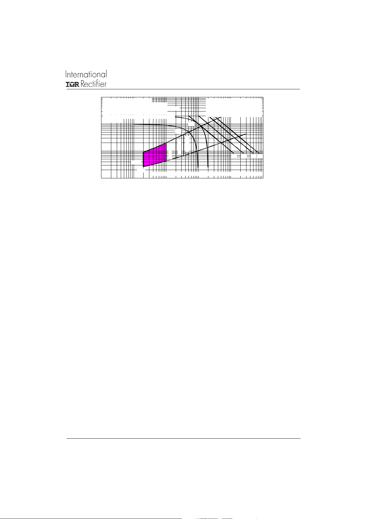
Rectangular gate pulse
a) Recommended load line for
rated di/dt : 20V, 10ohms; tr<=1 µs
b) Recommended load line for
<=30% rated di/dt : 10V, 10ohms
tr<=1 µs
10
(b)
Tj=-40 °C
Tj=25 °C
Tj=125 °C
1
Instantaneous Gate Voltage (V)
0.1
0.00 1 0.01 0. 1 1 1 0 100
VGD
IGD
Device: ST333C..L Series Frequency Limited by PG(AV)
Instantane ous Ga te Current
Fig. 17 - Gate Characteristics
(1) PGM = 10W, tp = 20ms
(2) PGM = 20W, tp = 10ms
(3) PGM = 40W, tp = 5ms
(4) PGM = 60W, tp = 3.3ms
(a)
(1)
(2)
ST333C..L Series
(3)
(4)
www.irf.com
9
 Loading...