

Bulletin I25200 rev. B 04/00
ST3230C..R SERIES
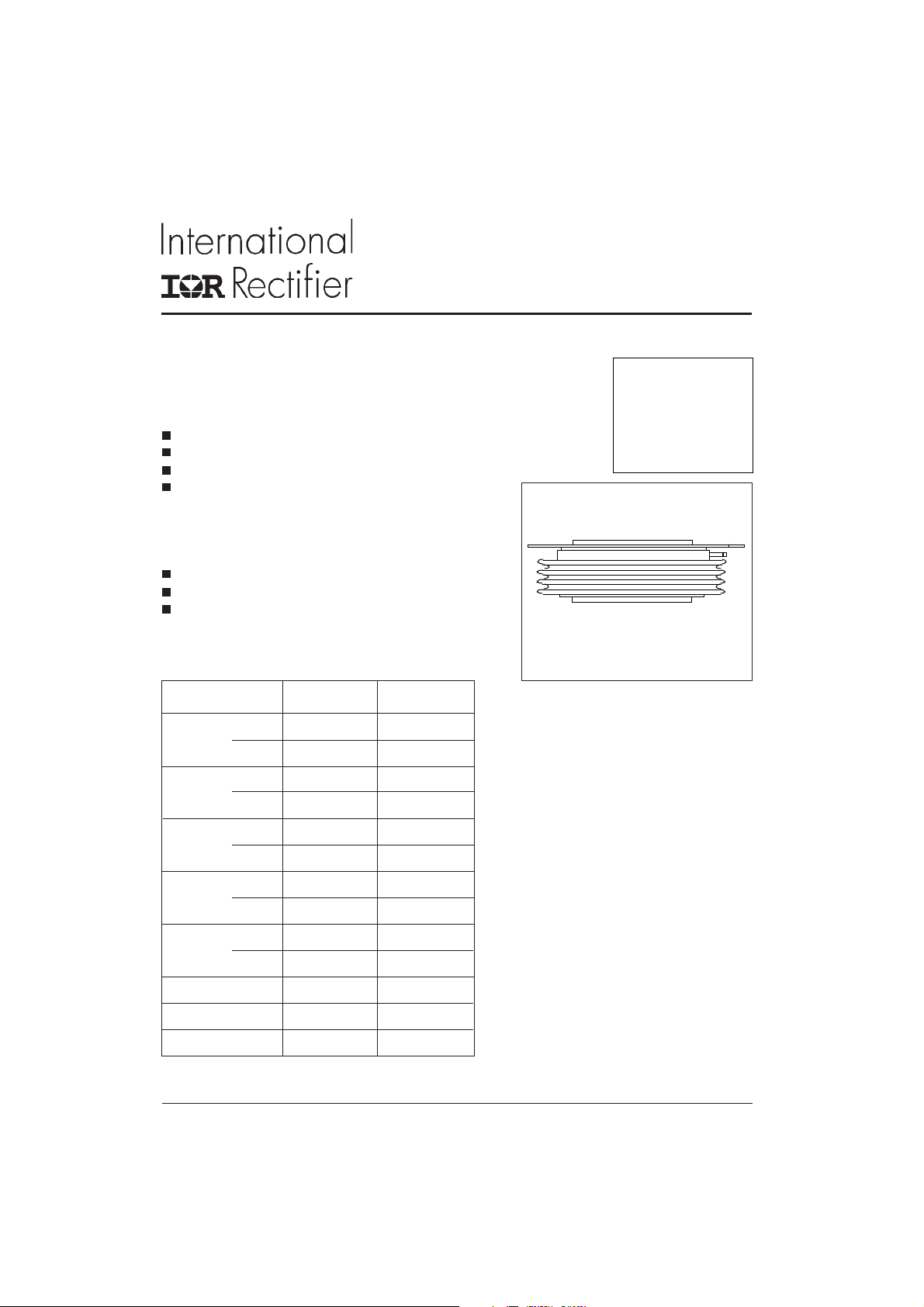
PHASE CONTROL THYRISTORS Hockey Puk Version
Features
Double side cooling
High surge capability
High mean current
Fatigue free
Typical Applications
DC motor controls
Controlled DC power supplies
AC controllers
Major Ratings and Characteristics
Parameters ST3230C..R Units
I
T(AV)
I
T(AV)
I
T(RMS)
I
TSM
@ T
C
@ T
hs
@ T
hs
@ 50Hz 61200 A
@ 60Hz 64000 A
2785 A
80 °C
3360 A
55 °C
5970 A
25 °C
3360A
(R-PUK)
I2t@
V
DRM/VRRM
t
q
T
J
50Hz 18730 KA2s
60Hz 17000 KA2s
@
typical 500 µs
max. 125 °C
www.irf.com
1000 to 1800 V
1
ST3230C..R Series
Bulletin I25200 rev. B 04/00
ELECTRICAL SPECIFICATIONS
Voltage Ratings
Voltage V
DRM/VRRM
Type number Code peak and off-state voltage repetitive peak voltage
10 1000 1100
12 1200 1300
ST3230C..R 250
14 1400 1500
16 1600 1700
18 1800 1900
On-state Conduction
Parameter ST3230C..R Units Conditions
I
Max. average on-state current 2785 (1720) A
T(AV)
@ Case temperature 80 °C
Max. average on-state current 3360 (1360) A
I
T(AV)
@ Heatsink temperature 55 (85) °C
Max. RMS on-state current 5970 A DC @ 25°C heatsink temperature double side cooled
I
T(RMS)
I
Max. peak, one-cycle No voltage
TSM
non-repetitive surge current reapplied
2
t Maximum I2t for fusing No voltage Initial TC = 125°C
I
V
Max. value of threshold voltage 0.92 V TJ = TJ max.
T(TO)
r
Max. value of on-state slope
t
resistance
Max. on-state voltage 1.3 V Ipk= 2900A, TC = 25°C
V
TM
Typical latching current 300 mA TJ = 25°C, VD = 5V
I
L
, max. repetitive V
, maximum non- I
RSM
DRM/IRRM
@ TC = 125°C
VVmA
180° conduction, half sine wave
double side (single side [anode side]) cooled
A
KA2s
mΩ
t = 10ms
t = 8.3ms
t = 10ms
t = 8.3ms
t = 10ms
t = 8.3ms
t = 10ms
t = 8.3ms
50% V
RRM
reapplied Sinusoidal half wave,
reapplied
50% V
RRM
reapplied
61200
64000
49000
51300
18730
17000
12000
10920
0.09 TJ = TJ max.
max.
Switching
Parameter ST3230C..R Units Conditions
di/dt Max. repetitive 50Hz (no repetitive) From 67% V
rate of rise of turned-on current to 1A, T
Maximum delay time 4.5
t
d
t
Typical turn-off time 500
q
150 (300) A/µs
µs
Gate drive 30V, 15Ω, Vd = 67% V
Rise time 0.5µs
I
= 1000A, tp = 1ms, TJ = TJ max, V
T
/dt = 2A/µs, V
dI
RR
2
to 1000A gate drive 10V, 5Ω, tr = 0.5µs
DRM
= TJ max.
J
67% V
DR =
DRM, dvDR
= 25°C
DRM, TJ
= 50V,
RM
/dt = 8V/µs linear
www.irf.com

Blocking
Parameter ST3230C..R Units Conditions
dv/dt Maximum linear rate of rise of
off-state voltage
I
Max. peak reverse and off-state
RRM
leakage current
I
DRM
Triggering
Parameter ST3230C..R Units Conditions
P
Maximum peak gate power 150 tp = 100µs
GM
P
Maximum average gate power 10
G(AV)
I
Max. peak positive gate current 30 A Anode positive with respect to cathode
GM
V
Max. peak positive gate voltage 30 V Anode positive with respect to cathode
GM
-V
Max. peak negative gate voltage 0.25 V Anode negative with respect to cathode
GM
I
Maximum DC gate current
GT
required to trigger
V
Maximum gate voltage required
GT
to trigger
V
DC gate voltage not to trigger 0.25 V TC = 125°C
GD
ST3230C..R Series
Bulletin I25200 rev. 04/00
500 V/µs TJ = TJ max. to 67% rated V
250 mA TJ = 125°C rated V
W
400 mA TC = 25°C, V
4VT
= 25°C, V
C
DRM/VRRM
= 5V
DRM
= 5V
DRM
Max. gate current/voltage not to
trigger is the max. value which
will not trigger any unit with rated
anode-to-cathode applied
V
DRM
DRM
applied
Thermal and Mechanical Specification
Parameter ST3230C..R Units Conditions
TJ max. Max. operating temperature 125 On-state (conducting)
Max. storage temperature range -55 t o 1 25
T
stg
R
Thermal resistance, junction 0.019 DC operation single side cooled
thJ-C
to case 0.0095 DC operation double side cooled
Thermal resistance, case 0.004 Single side cooled
R
th(C-h)
to heatsink 0.002 Double side cooled
F Mounting force ± 10%
43000
(4400)
wt Approximate weight 1600 g
Case style (R-PUK) See Outline Table
∆R
Conduction
thJ-C
(The following table shows the increment of thermal resistence R
°C
K/W
K/W
N
(Kg)
when devices operate at different conduction angles than DC)
thJ-C
Conduction angle Single side Double side Units Conditions
180° 0.0010 0.0010 T
120° 0.0017 0.0017 K/W
60° 0.0044 0.0044
J
www.irf.com
Clamping force 43KN with
mounting compound
= TJ max.
3

ST3230C..R Series
Bulletin I25200 rev. B 04/00
Ordering Information Table
Device Code
ST 323 0 C 18 R 1
1 - Thyristor
2 - Essential part number
3 - 0 = Converter grade
4 - C = Ceramic Puk
5 - Voltage code: Code x 100 = V
6 - R = Puk Case
7 - 0 = Eyelet terminals (Gate and Auxiliary Cathode Unsoldered Leads)
8 - Critical dv/dt: None = 500V/µsec (Standard selection)
Outline Table
51 2 3
4
(See Voltage Rating Table)
RRM
7
6 8
1 = Fast-on terminals (Gate and Auxiliary Cathode Unsoldered Leads)
2 = Eyelet terminals (Gate and Auxiliary Cathode Soldered Leads)
3 = Fast-on terminals (Gate and Auxiliary Cathode Soldered Leads)
L = 1000V/µsec (Special selection)
112.5 (4.4) DIA. MAX.
73.2 (2.9) DIA. MAX.
TWO PLACES
GATE
1.5 (0.06) DIA.
37.7 (1.5 ) MA X.
ANODE
CATHODE
HOLE 1.5 (0.06)
DIA. MAX.
4.76 (0.2)
3.7 (0.15) DIA. NOM. X
2.1 (0.1) DEEP MIN.
BOTH ENDS
4
20° ± 5°
)
4
2
.
0
(
3
.
6
(R-PUK)
All dimensions in millimeters (inches)
Quote between upper and lower
pole pieces has to be considered
after application of Mounting Force
(see Thermal and Mechanical
Specification)
www.irf.com
ST3230C..R Series
Bulletin I25200 rev. B 04/00
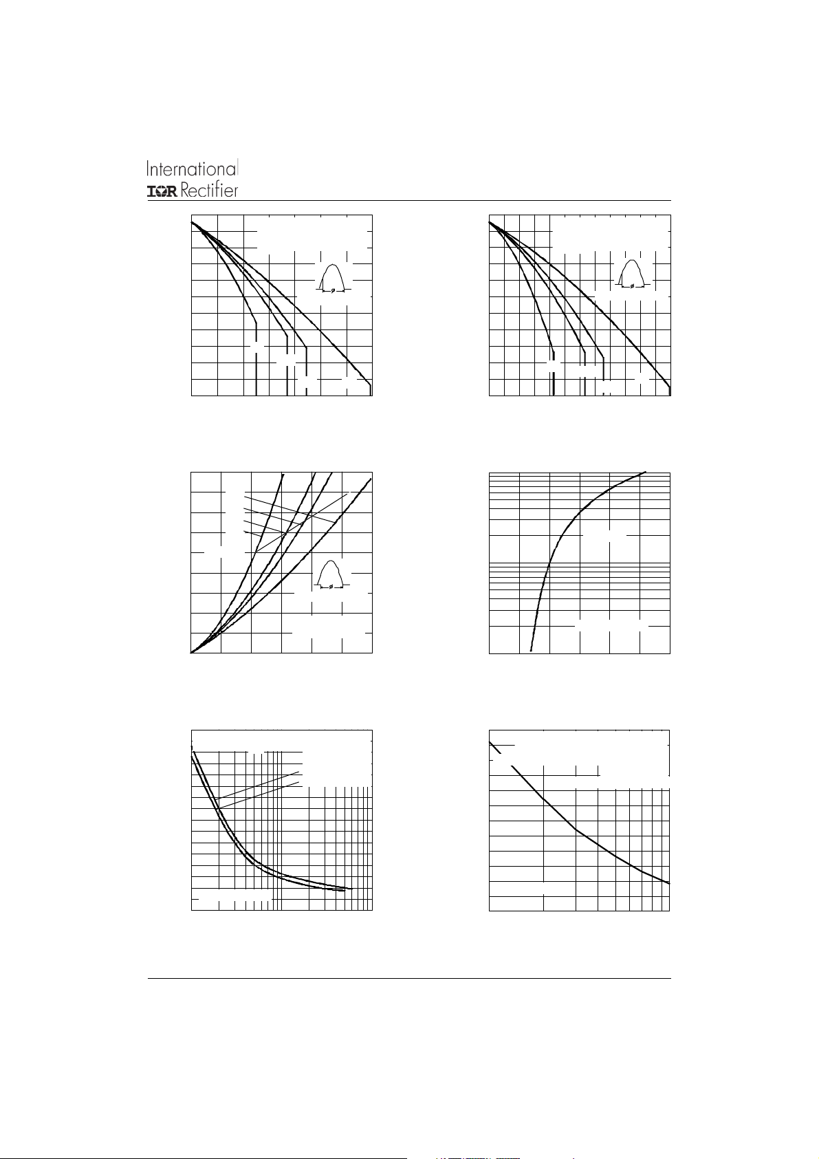
130
120
110
ST3230C ..R Se ries
(Single Side Cooled)
R (D C ) = 0.023 K/W
th J-hs
100
90
80
Cond uction A ngle
70
60
50
40
30
20
0 500 1000 1500 2000 2500 3000 3500
Maxim um Allowable Heatsink Tem perature (°C)
60°
120°
180°
DC
A vera g e O n -sta te C urre n t (A)
Fig. 1 - Current Ratings Characteristics Fig. 2 - Current Ratings Characteristics
9000
8000
7000
6000
5000
DC
180°
120°
60°
RMS Limit
4000
3000
2000
1000
0
Maximum Average On-state Power Loss (W)
0 1000 2000 3000 4000 5000 6000
Con duc tion Angle
ST3230C..R Series
T = 125 °C
J
Average On-state Current (A)
Fig. 3 - On-state Power Loss Characteristics
130
120
110
ST3230C ..R Series
(Double Side Cooled)
R (DC) = 0.0115 K/W
th J-hs
100
90
80
70
60
50
40
60°
30
20
0 1000 2000 3000 4000 5000 6000
Maximum Allowable Heatsink Temperature (°C)
Average On-state Current (A)
10000
1000
ST3230C ..R Se ries
Ins ta n ta n e o u s O n -st a te C u rre n t ( A )
100
0.511.52
In stan ta ne ou s O n -st a te Vo ltag e (V )
Fig. 4 - On-state Voltage Drop Characteristics
Conduction Angle
120°
180°
T = 125° C
J
DC
55000
At Any Rated Load Condition And With
5 0 % R a t e d V A p p li e d F o llo w in g Su rg e
50000
RRM
45000
40000
35000
30000
Init ial T = 1 25° C
J
@ 60 H z 0.0083 s
@ 50 H z 0.0100 s
100000
M axim u m N o n Re pe titiv e Su rg e C u rre nt
V ersu s P u lse Tra in Du ra t ion . C o ntro l
O f C on d u ctio n M a y N o t Be M a in ta in e d .
90000
80000
50% Rate d V Rea p p lied
70000
60000
Initia l T = 12 5 ° C
RRM
25000
Peak Half Sine Wave On-state Current (A)
50000
40000
ST3230C ..R Se ries
110
Pulse Tra in Du ra tio n (m s)
20000
Peak Half Sine Wave On-state Current (A)
ST3230C ..R Se ries
15000
110100
Number O f Equal Amplitude Half Cycle Current Pulses (N)
Fig. 5 - Maximum Non-Repetitive Surge Current Fig. 6 - Maximum Non-Repetitive Surge Current
www.irf.com
J
5

ST3230C..R Series
Bulletin I25200 rev. B 04/00
10000
ST3230C ..R Series
T = 125° C
J
I = 1000A
T
1000
I
T
p
t = 3ms
dI
dt
T
Tota l stor ed c h ar ge - Qrr ( µC )
100
0.1 1 10 100
Rate Of Decay Of On-state Current - di/dt (A/µs)
Fig. 7 - Stored Charged
0.1
Ste ady St a te Value
R = 0.019 K/W
thJ-C
thJ-C
(Single Side Coo le d )
R = 0.0095 K/W
0.01
thJ-C
(Dou ble Side C o ole d)
(D C O p e ration)
0.001
ST3230C ..R S eries
0.00 01
Transien t The rm al Im p e da nc e Z (K/W )
0.001 0.01 0.1 1 10 100
Square W ave P ulse D u ra tion (s)
100
Fig. 8 - Thermal Impedance Z
(1) PG M = 2W
Characteristics
thJ-C
(2) PG M = 4W
(3) PG M = 8W
(4) PG M = 20W
(5) PG M = 50W
10
(6) PGM =100W
1
VG D
Tj=-40 °C
Tj=25 °C
Tj=1 25 °C
(1)
(5)
(2)
IG D
Instan ta n eo us Gat e V o ltage (V )
Device: ST3230C..R Series
0.1
0.001 0.01 0.1 1 10
Frequen cy Limited by PG(AV)
Instan tane ou s G ate C u rren t (A )
rr
Q
I ( REC )
RM
(6)
(3) (4)
t
Fig. 9 - Gate Characteristics
6
www.irf.com
 Loading...