

ST300CLPbF Series
Vishay High Power Products
Phase Control Thyristors
(Hockey PUK Version), 560 A
FEATURES
• Center amplifying gate
• Metal case with ceramic insulator
• International standard case TO-200AC (B-PUK)
• Lead (Pb)-free
TO-200AC (B-PUK)
PRODUCT SUMMARY
I
T(AV)
560 A
MAJOR RATINGS AND CHARACTERISTICS
PARAMETER TEST CONDITIONS VALUES UNITS
I
T(AV)
I
T(RMS)
I
TSM
2
I
t
V
DRM/VRRM
t
q
T
J
T
hs
T
hs
50 Hz 8000
60 Hz 8380
50 Hz 320
60 Hz 292
Typical 100 µs
• Designed and qualified for industrial level
TYPICAL APPLICATIONS
• DC motor controls
• Controlled DC power supplies
• AC controllers
560 A
55 °C
1115 A
25 °C
A
kA2s
400 to 2000 V
- 40 to 125 °C
RoHS
COMPLIANT
ELECTRICAL SPECIFICATIONS
VOLTAGE RATINGS
V
TYPE NUMBER
ST300C..L
Document Number: 94405 For technical questions, contact: ind-modules@vishay.com
Revision: 11-Aug-08 1
VOLTAGE
CODE
04 400 500
08 800 900
12 1200 1300
16 1600 1700
18 1800 1900
20 2000 2100
DRM/VRRM
PEAK AND OFF-STATE VOLTAGE
, MAXIMUM REPETITIVE
V
V
, MAXIMUM NON-REPETITIVE
RSM
PEAK VOLTAGE
V
I
DRM/IRRM
AT T
= TJ MAXIMUM
J
www.vishay.com
MAXIMUM
mA
50
ST300CLPbF Series
Vishay High Power Products
Phase Control Thyristors
(Hockey PUK Version), 560 A
ABSOLUTE MAXIMUM RATINGS
PARAMETER SYMBOL TEST CONDITIONS VALUES UNITS
Maximum average on-state current
at heatsink temperature
Maximum RMS on-state current I
I
T(RMS)
Maximum peak, one-cycle
non-repetitive surge current
2
Maximum I
Maximum I
t for fusing I2t
2
√t for fusing I2√t t = 0.1 to 10 ms, no voltage reapplied 3200 kA2√s
Low level value of threshold voltage V
High level value of threshold voltage V
Low level value of on-state slope resistance r
High level value of on-state slope resistance r
Maximum on-state voltage V
Maximum holding current I
Typical latching current I
T(AV)
180° conduction, half sine wave
double side (single side) cooled
DC at 25 °C heatsink temperature double side cooled 1115
I
TSM
T(TO)1
T(TO)2
t1
t2
TM
H
L
t = 10 ms
t = 8.3 ms 8380
t = 10 ms
t = 8.3 ms 7040
t = 10 ms
t = 8.3 ms 292
t = 10 ms
t = 8.3 ms 207
(16.7 % x π x I
(I > π x I
(16.7 % x π x I
(I > π x I
Ipk = 1635 A, TJ = TJ maximum, tp = 10 ms sine pulse 2.18 V
TJ = 25 °C, anode supply 12 V resistive load
No voltage
reapplied
100 % V
reapplied
No voltage
RRM
Sinusoidal half wave,
initial T
= TJ maximum
J
reapplied
100 % V
RRM
reapplied
< I < π x I
T(AV)
), TJ = TJ maximum 0.98
T(AV)
< I < π x I
T(AV)
), TJ = TJ maximum 0.73
T(AV)
), TJ = TJ maximum 0.97
T(AV)
), TJ = TJ maximum 0.74
T(AV)
560 (275) A
55 (75) °C
8000
6730
320
226
600
1000
A
kA2s
V
mΩ
mA
SWITCHING
PARAMETER SYMBOL TEST CONDITIONS VALUES UNITS
Maximum non-repetitive rate of rise
of turned-on current
Typical delay time t
Typical turn-off time t
dI/dt
d
q
Gate drive 20 V, 20 Ω, t
T
= TJ maximum, anode voltage ≤ 80 % V
J
≤ 1 µs
r
DRM
Gate current 1 A, dIg/dt = 1 A/µs
V
= 0.67 % V
d
, TJ = 25 °C
DRM
ITM = 550 A, TJ = TJ maximum, dI/dt = 40 A/µs,
V
= 50 V, dV/dt = 20 V/µs, gate 0 V 100 Ω, tp = 500 µs
R
1000 A/µs
1.0
µs
100
BLOCKING
PARAMETER SYMBOL TEST CONDITIONS VALUES UNITS
Maximum critical rate of rise of
off-state voltage
Maximum peak reverse and
off-state leakage current
dV/dt T
I
RRM,
I
DRM
= TJ maximum linear to 80 % rated V
J
TJ = TJ maximum, rated V
DRM/VRRM
DRM
500 V/µs
applied 50 mA
www.vishay.com For technical questions, contact: ind-modules@vishay.com
Document Number: 94405
2 Revision: 11-Aug-08
ST300CLPbF Series
Phase Control Thyristors
Vishay High Power Products
(Hockey PUK Version), 560 A
TRIGGERING
DRM
VALUES
TYP. MAX.
20
5.0
200 -
10.0 mA
0.25 V
UNITS
mAT
PARAMETER SYMBOL TEST CONDITIONS
Maximum peak gate power P
Maximum average gate power P
Maximum peak positive gate current I
Maximum peak positive gate voltage + V
Maximum peak negative gate voltage - V
G(AV)
GM
TJ = TJ maximum, tp ≤ 5 ms 10.0
GM
TJ = TJ maximum, f = 50 Hz, d% = 50 2.0
TJ = TJ maximum, tp ≤ 5 ms 3.0 A
GM
TJ = TJ maximum, tp ≤ 5 ms
GM
TJ = - 40 °C
DC gate current required to trigger I
DC gate voltage required to trigger V
DC gate current not to trigger I
DC gate voltage not to trigger V
GT
GT
GD
GD
= 25 °C 100 200
J
T
= 125 °C 50 -
J
TJ = - 40 °C 2.5 -
= 25 °C 1.8 3.0
T
J
= 125 °C 1.1 -
T
J
Maximum required gate trigger/
current/voltage are the lowest
value which will trigger all units
12 V anode to cathode applied
Maximum gate current/
voltage not to trigger is the
TJ = TJ maximum
maximum value which will not
trigger any unit with rated V
anode to cathode applied
W
V
V
THERMAL AND MECHANICAL SPECIFICATIONS
PARAMETER SYMBOL TEST CONDITIONS VALUES UNITS
Maximum operating junction temperature range T
Maximum storage temperature range T
Maximum thermal resistance, junction to heatsink R
Maximum thermal resistance, case to heatsink R
J
Stg
thJ-hs
thC-hs
DC operation single side cooled 0.11
DC operation double side cooled 0.05
DC operation single side cooled 0.011
DC operation double side cooled 0.006
Mounting force, ± 10 %
Approximate weight 250 g
Case style See dimensions - link at the end of datasheet TO-200AC (B-PUK)
ΔR
CONDUCTION ANGLE
CONDUCTION
thJ-hs
SINUSOIDAL CONDUCTION RECTANGULAR CONDUCTION
SINGLE SIDE DOUBLE SIDE SINGLE SIDE DOUBLE SIDE
TEST CONDITIONS UNITS
180° 0.012 0.010 0.008 0.008
120° 0.014 0.015 0.014 0.014
90° 0.018 0.018 0.019 0.019
= TJ maximum K/W
T
J
60° 0.026 0.027 0.027 0.028
30° 0.045 0.046 0.046 0.046
Note
• The table above shows the increment of thermal resistance R
when devices operate at different conduction angles than DC
thJ-hs
- 40 to 125
- 40 to 150
9800
(1000)
°C
K/W
N
(kg)
Document Number: 94405 For technical questions, contact: ind-modules@vishay.com
www.vishay.com
Revision: 11-Aug-08 3
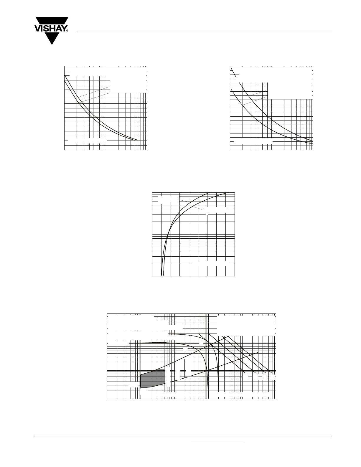
ST300CLPbF Series
Vishay High Power Products
130
120
110
100
90
80
70
60
50
40
30
0 100 200 300 400 500
Maximum Allowable Heatsink Temperature (°C)
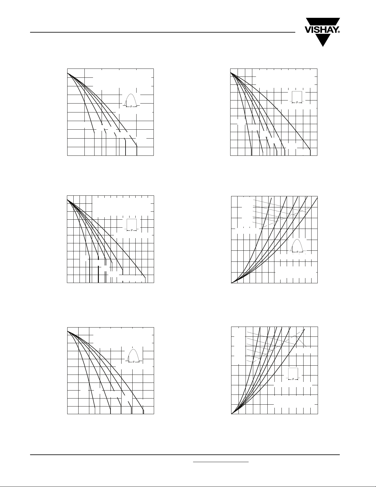
Fig. 1 - Current Ratings Characteristics
130
120
110
100
90
80
70
60
50
40
30
20
0 100 200 300 400 500 600 700
Maximum Allowable Heatsink Temperature (°C)
Fig. 2 - Current Ratings Characteristics
ST300C..L Series
(Single Side Cooled)
R (DC) = 0.11 K/W
thJ-hs
Conduction Angle
30°
60°
90°
120°
Average On-state Current (A)
ST300C..L Series
(Single Side Cooled)
R (DC) = 0.11 K/W
thJ-hs
Conduction Period
30°
60°
90°
120°
180°
Average On-state Current (A)
Phase Control Thyristors
(Hockey PUK Version), 560 A
130
120
110
100
180°
Maximum Allowable Heatsink Temperature (°C)
1600
1400
1200
1000
800
600
400
200
DC
Maximum Average On-state Power Loss (W)
ST300C..L Series
(Double Side Cooled)
R (DC) = 0.05 K/W
thJ-hs
90
80
Conduction Period
70
30°
60
50
40
30
20
60°
90°
120°
180°
DC
0 200 400 600 800 1000 1200
Average On-state Current (A)
Fig. 4 - Current Ratings Characteristics
180°
120°
90°
60°
30°
RMS Limit
Conduction Angle
ST300C..L Series
T = 125 °C
J
0
0 100 200 300 400 500 600 700
Average On-state Current (A)
Fig. 5 - On-State Power Loss Characteristics
130
120
110
ST300C..L Series
(Double Side Cooled)
R (DC) = 0.05 K/W
thJ-hs
100
90
80
Conduction Angle
70
60
50
40
30
30°
60°
90°
120°
180°
20
0 200 400 600 800
Maximum Allowable Heatsink Temperature (°C)
www.vishay.com For technical questions, contact: ind-modules@vishay.com
4 Revision: 11-Aug-08
Average On-state Current (A)
Fig. 3 - Current Ratings Characteristics
1800
1600
1400
1200
1000
DC
180°
120°
90°
60°
30°
RMS Limit
800
600
400
200
0
Maximum Average On-state Power Loss (W)
0 200 400 600 800 1000 1200
Average On-state Current (A)
Fig. 6 - On-State Power Loss Characteristics
Conduction Period
ST300C..L Series
T = 125 °C
J
Document Number: 94405
ST300CLPbF Series
Phase Control Thyristors
(Hockey PUK Version), 560 A
7500
7000
6500
6000
5500
5000
4500
4000
3500
Peak Half Sine Wave On-state Current (A)
3000
Number Of Equal Amplitude Half Cycle Current Pulses (N)
At Any Rated Load Condition And With
Rated Vrrm Applied Following Surge.
ST300C..L Series
Initial Tj = 125 °C
@ 60 Hz 0.0083 s
@ 50 Hz 0.0100 s
110100
Fig. 7 - Maximum Non-Repetitive Surge Current
Single and Double Side Cooled
10000
)A( tnerruC etats-nO suoenatnatsnI
T = 25 °C
J
Vishay High Power Products
8000
Maximum Non Repetitive Surge Current
7500
7000
6500
6000
5500
5000
4500
4000
3500
3000
Peak Half Sine Wave On-state Current (A)
Fig. 8 - Maximum Non-Repetitive Surge Current
T = 125 °C
J
Versus Pulse Train Duration. Control
Of Conduction May Not Be Maintained.
Initial Tj = 125 °C
No Voltage Reapplied
Rated Vrrm Reapplied
ST300C..L Series
0.01 0.1 1
Pulse Train Duration (s)
Single and Double Side Cooled
1000
ST300C..L Series
100
0123456789
Instantaneous On-state Voltage (V)
Fig. 9 - On-State Voltage Drop Characteristcs
100
Rectangular gate pulse
a) Recommended load line for
(K/W)
rated di/dt : 20V, 10ohms; tr<=1 μs
thJ-hs
b) Recommended load line for
<=30% rated di/dt : 10V, 10ohms
10
tr<=1 μs
1
Tj=125
°C
(a)
(b)
Tj=-40
Tj=25 °C
°C
(1) PGM = 10W, tp = 4ms
(2) PGM = 20W, tp = 2ms
(3) PGM = 40W, tp = 1ms
(4) PGM = 60W, tp = 0.66ms
(1)
(2) (3)
VGD
IGD
Transient Thermal Impedance Z
0.1
Device: ST300C..L Series
Frequency Limited by PG(AV)
0.001 0.01 0.1 1 10 100
Square Wave Pulse Duration (s)
Fig. 10 - Thermal Impedance Z
Characteristics
thJ-hs
(4)
Document Number: 94405 For technical questions, contact: ind-modules@vishay.com
Revision: 11-Aug-08 5
www.vishay.com
ST300CLPbF Series
Vishay High Power Products
1
Steady State Value
R = 0.11 K/W
thJ-hs
(Single Side Cooled)
0.1
R = 0.05 K/W
thJ-hs
(Double Side Cooled)
(DC Operation)
0.01
Instantaneous Gate Voltage (V)
0.001
0.001 0.01 0.1 1 10
ORDERING INFORMATION TABLE
Phase Control Thyristors
(Hockey PUK Version), 560 A
ST300C..L Series
Instantaneous Gate Current (A)
Fig. 11 - Gate Characteristics
Device code
ST 30 0 C 20 L 1 - PbF
324
1
- Thyristor
2
- Essential part number
3
- 0 = Converter grade
4
- C = Ceramic PUK
5
- Voltage code x 100 = V
6
- L = PUK case TO-200AC (B-PUK)
7
- 0 = Eyelet terminals (gate and auxiliary cathode unsoldered leads)
51
6789
(see Voltage Ratings table)
RRM
1 = Fast-on terminals (gate and auxiliary cathode unsoldered leads)
2 = Eyelet terminals (gate and auxiliary cathode soldered leads)
3 = Fast-on terminals (gate and auxiliary cathode soldered leads)
8
- Critical dV/dt:
None = 500 V/µs (standard selection)
L = 1000 V/µs (special selection)
9
- Lead (Pb)-free
LINKS TO RELATED DOCUMENTS
Dimensions http://www.vishay.com/doc?95076
www.vishay.com For technical questions, contact: ind-modules@vishay.com
6 Revision: 11-Aug-08
Document Number: 94405

Legal Disclaimer Notice
Vishay
Notice
The products described herein were acquired by Vishay Intertechnology, Inc., as part of its acquisition of
International Rectifier’s Power Control Systems (PCS) business, which closed in April 2007. Specifications of the
products displayed herein are pending review by Vishay and are subject to the terms and conditions shown below.
Specifications of the products displayed herein are subject to change without notice. Vishay Intertechnology, Inc., or
anyone on its behalf, assumes no responsibility or liability for any errors or inaccuracies.
Information contained herein is intended to provide a product description only. No license, express or implied, by
estoppel or otherwise, to any intellectual property rights is granted by this document. Except as provided in Vishay's
terms and conditions of sale for such products, Vishay assumes no liability whatsoever, and disclaims any express
or implied warranty, relating to sale and/or use of Vishay products including liability or warranties relating to fitness
for a particular purpose, merchantability, or infringement of any patent, copyright, or other intellectual property right.
The products shown herein are not designed for use in medical, life-saving, or life-sustaining applications.
Customers using or selling these products for use in such applications do so at their own risk and agree to fully
indemnify Vishay for any damages resulting from such improper use or sale.
International Rectifier
are registered trademarks of International Rectifier Corporation in the U.S. and other countries. All other product
names noted herein may be trademarks of their respective owners.
®
, IR®, the IR logo, HEXFET®, HEXSense®, HEXDIP®, DOL®, INTERO®, and POWIRTRAIN
®
Document Number: 99901 www.vishay.com
Revision: 12-Mar-07 1

DIMENSIONS in millimeters (inches)
Outline Dimensions
Vishay High Power Products
TO-200AC (B-PUK)
Case Style TO-200AC (B-PUK)
Creepage distance: 36.33 (1.430) minimum
Strike distance: 17.43 (0.686) minimum
0.7 (0.03) MIN.
27 (1.06) MAX.
0.7 (0.03) MIN.
34 (1.34) DIA. MAX.
2 places
53 (2.09) DIA. MAX.
58.5 (2.3) DIA. MAX.
6.2 (0.24) MIN.
Pin receptacle
AMP. 60598-1
4.7 (0.18)
20° ± 5°
36.5 (1.44)
2 holes DIA. 3.5 (0.14) x 2.5 (0.1) deep
Quote between upper and lower pole pieces has to be considered after
application of mounting force (see thermal and mechanical specification)
Document Number: 95076 For technical questions concerning discrete products, contact: diodes-tech@vishay.com
Revision: 01-Aug-07 For technical questions concerning module products, contact: ind-modules@vishay.com
www.vishay.com
1
 Loading...