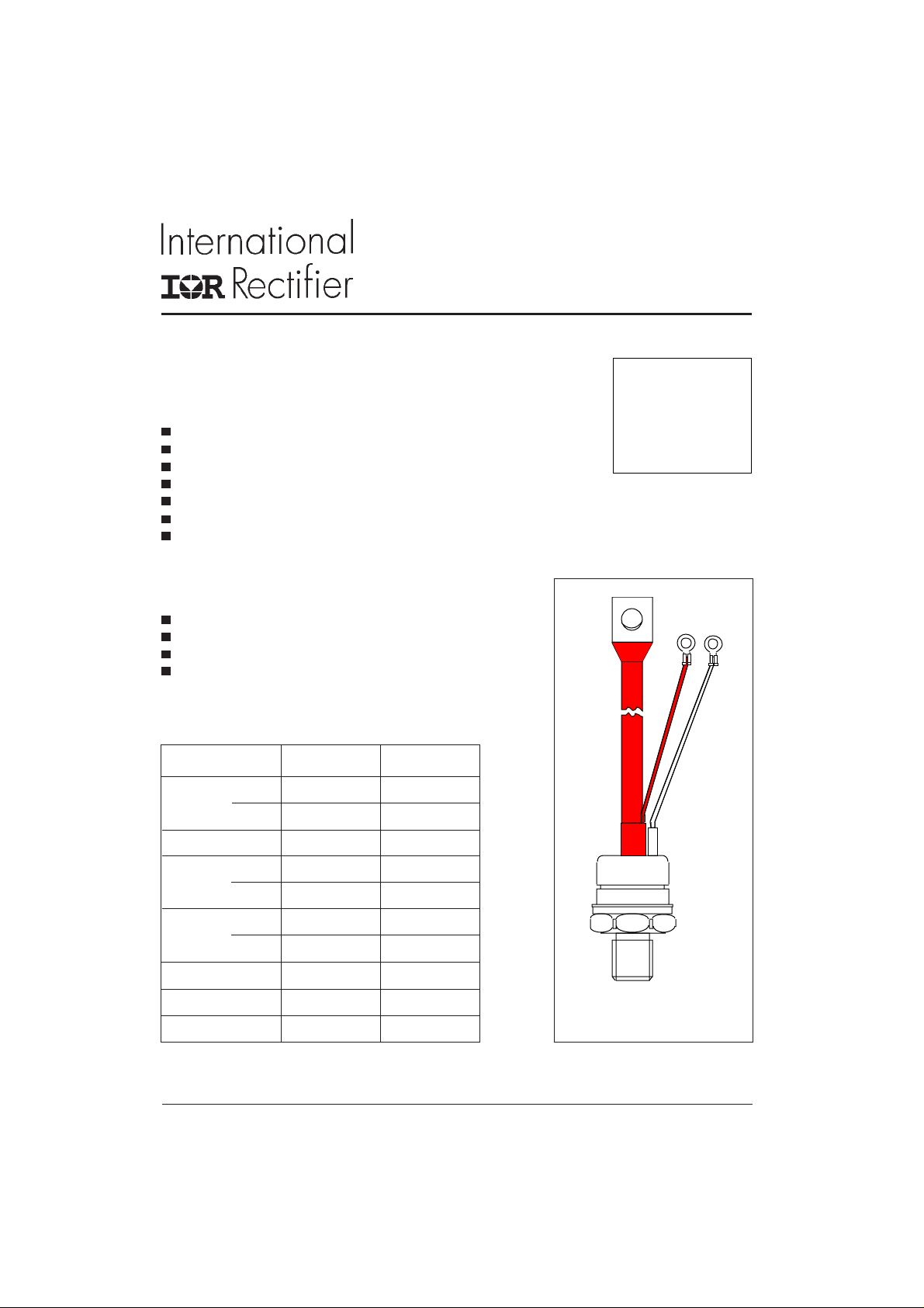
Vishay ST223S SERIES Data Sheet

Bulletin I25175 rev. C 12/96
ST223S SERIES
INVERTER GRADE THYRISTORS
Features
All diffused design
Center amplifying gate
Guaranteed high dv/dt
Guaranteed high di/dt
High surge current capability
Low thermal impedance
High speed performance
Typical Applications
Inverters
Choppers
Induction heating
All types of force-commutated converters
Major Ratings and Characteristics
Parameters ST223S Units
I
T(AV)
I
T(RMS)
I
TSM
@ T
C
@ 50Hz 5850 A
@ 60Hz 6120 A
220 A
85 °C
345 A
Stud Version
220A
I2t@
V
DRM/VRRM
range 10 to 20 µs
t
q
T
J
50Hz 171 KA2s
@ 60Hz 156 KA
400 to 800 V
- 40 to 125 °C
www.irf.com
2
s
case style
TO-209AB (TO-93)
1

ST223S Series
Bulletin I25175 rev. C 12/96
ELECTRICAL SPECIFICATIONS
Voltage Ratings
Voltage V
DRM/VRRM
Type number Code repetitive peak voltage non-repetitive peak voltage @ T
ST223S 40
04 400 500
08 800 900
Current Carrying Capability
, maximum V
, maximum I
RSM
DRM/IRRM
VVmA
max.
= TJ max.
J
I
Frequency Units
180
TM
o
el
180oel
I
TM
I
TM
100µs
50Hz 630 430 970 690 6450 4850
400Hz 630 420 1010 71 0 3140 2280
1000Hz 580 370 1000 680 1860 1310 A
2500Hz 420 250 860 630 980 790
Recovery voltage Vr 50 50 50 50 50 50
Voltage before turn-on Vd V
DRM
V
DRM
V
DRM
Rise of on-state current di/dt 50 5 0 - - - - A/µs
Case temperature 60 85 60 85 60 85 °C
Equivalent values for RC circuit 47Ω / 0.22µF 47Ω / 0.22µF 47Ω / 0.22µF
On-state Conduction
Parameter ST223S Units Conditions
I
Max. average on-state current 220 A 180° conduction, half sine wave
T(AV)
@ Case temperature 85 °C
I
Max. RMS on-state current 345 DC @ 76°C case temperature
T(RMS)
I
Max. peak, one half cycle, 5850 t = 10ms No voltage
TSM
non-repetitive surge current 6120 A t = 8.3ms reapplied
4920 t = 10ms 100% V
5150 t = 8.3ms reapplied Sinusoidal half wave,
2
t Maximum I2t for fusing 171 t = 10ms No voltage Initial TJ = TJ max
I
156 t = 8.3ms reapplied
121 t = 10ms 100% V
KA2s
111 t = 8.3ms reapplied
2
I
√t Maximum I2√t for fusing 1710 KA2√s t = 0.1 to 10ms, no voltage reapplied
RRM
RRM
V
2
www.irf.com

ST223S Series
Bulletin I25175 rev. C 12/96
On-state Conduction
Parameter ST223S Units Conditions
VTMMax. peak on-state voltage 1.58 ITM= 600A, TJ = TJ max, tp = 10ms sine wave pulse
Low level value of threshold
V
T(TO)1
voltage
High level value of threshold
V
T(TO)2
voltage
Low level value of forward
r
t1
slope resistance
High level value of forward
r
t2
slope resistance
Maximum holding current 600 TJ = 25°C, IT > 30A
I
H
Typical latching current 1000 TJ = 25°C, VA= 12V, Ra = 6Ω, IG= 1A
I
L
Switching
Parameter ST223S Units Conditions
di/dt Max. non-repetitive rate of rise T
of turned-on current I
t
Typical delay time 0.78
d
Max. turn-off time 10 20
t
q
1.05 (16.7% x π x I
V
1.09 (I > π x I
0.88 (16.7% x π x I
mΩ
0.82 (I > π x I
mA
= TJ max, V
1000 A/µs
Min Max
J
= 2 x di/dt
TM
= 25°C, V
T
J
Resistive load, Gate pulse: 10V, 5Ω source
µs
T
= TJ max, I
J
= 50V, tp = 500µs, dv/dt: see table in device code
V
R
< I < π x I
T(AV)
), TJ = TJ max.
T(AV)
< I < π x I
T(AV)
), TJ = TJ max.
T(AV)
DRM
= rated V
DM
= 300A, commutating di/dt = 20A/µs
TM
= rated V
DRM, ITM
T(AV)
T(AV)
DRM
), TJ = TJ max.
), TJ = TJ max.
= 50A DC, tp= 1µs
Blocking
Parameter ST223S Units Conditions
dv/dt Maximum critical rate of rise of T
off-state voltage available on request
Max. peak reverse and off-state
I
RRM
leakage current
I
DRM
500 V/µs
40 mA T
Triggering
Parameter ST223S Units Conditions
PGMMaximum peak gate power 60
Maximum average gate power 10
P
G(AV)
I
Max. peak positive gate current 10 A TJ = TJ max, tp ≤ 5ms
GM
+VGMMaximum peak positive
gate voltage
Maximum peak negative
-V
GM
gate voltage
Max. DC gate current required
I
GT
to trigger
V
Max. DC gate voltage required
GT
to trigger
Max. DC gate current not to trigger 20 mA
I
GD
V
Max. DC gate voltage not to trigger 0.25 V
GD
20
5
200 m A
3V
WTJ = TJ max, f = 50Hz, d% = 50
VTJ = TJ max, tp ≤ 5ms
T
TJ = TJ max, rated V
www.irf.com
= TJ max., linear to 80% V
J
= TJ max., rated V
J
= 25°C, VA = 12V, Ra = 6Ω
J
DRM/VRRM
applied
DRM
, higher value
DRM
applied
3
 Loading...