Vishay ST180SPbF Series Data Sheet

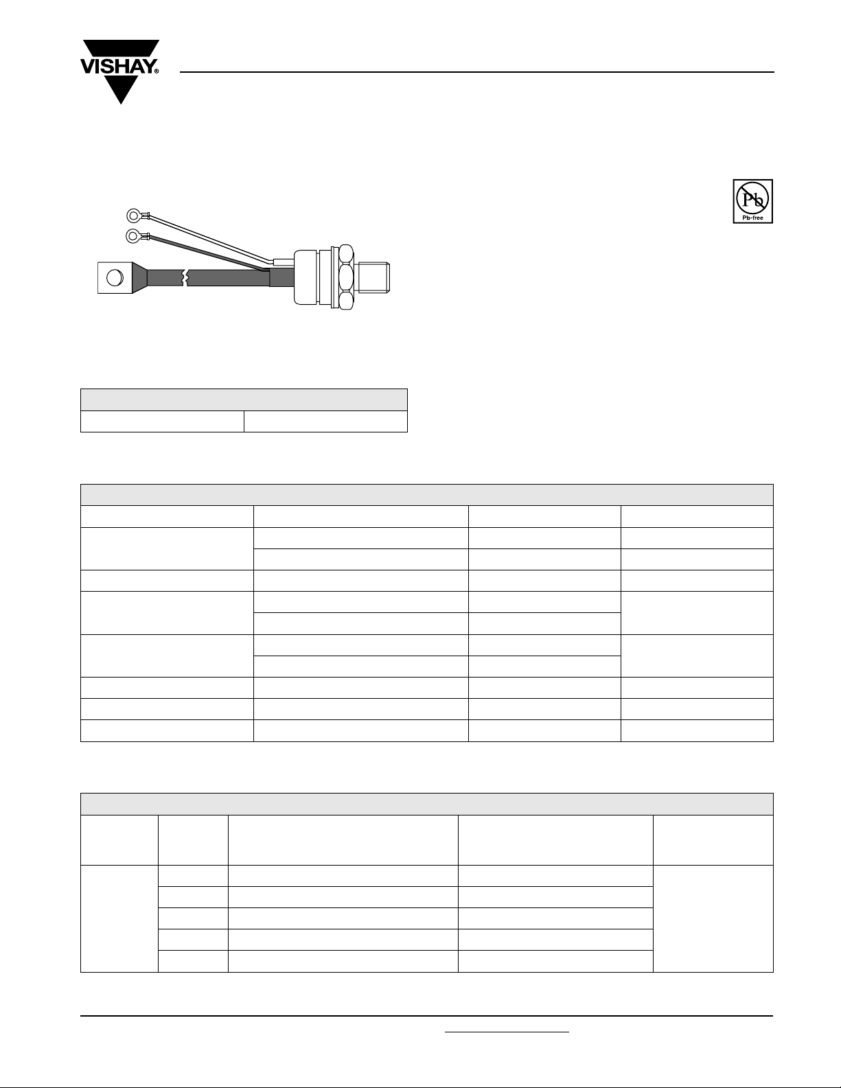
TO-209AB (TO-93)
PRODUCT SUMMARY
I
T(AV)
Vishay High Power Products
Phase Control Thyristors
(Stud Version), 200 A
FEATURES
• Center amplifying gate
• International standard case TO-209AB (TO-93)
• Hermetic metal case with ceramic insulator
(Also available with glass-metal seal up to 1200 V)
• Compression bonded encapsulation for heavy duty
operations such as severe thermal cycling
• Lead (Pb)-free
• Designed and qualified for industrial level
TYPICAL APPLICATIONS
• DC motor controls
200 A
• Controlled DC power supplies
• AC controllers
ST180SPbF Series
RoHS
COMPLIANT
MAJOR RATINGS AND CHARACTERISTICS
PARAMETER TEST CONDITIONS VALUES UNITS
I
T(AV)
I
T(RMS)
I
TSM
2
I
t
V
DRM/VRRM
t
q
T
J
T
C
50 Hz 5000
60 Hz 5230
50 Hz 125
60 Hz 114
Typical 100 µs
200 A
85 °C
314 A
400 to 2000 V
- 40 to 125 °C
ELECTRICAL SPECIFICATIONS
VOLTAGE RATINGS
TYPE
NUMBER
ST180S
V
VOLTAGE
CODE
04 400 500
08 800 900
12 1200 1300
16 1600 1700
20 2000 2100
DRM/VRRM
, MAXIMUM REPETITIVE PEAK
AND OFF-STATE VOLTAGE
V
V
, MAXIMUM
NON-REPETITIVE PEAK VOLTAGE
RSM
V
I
DRM/IRRM
AT T
A
kA2s
MAXIMUM
= TJ MAXIMUM
J
mA
30
Document Number: 94397 For technical questions, contact: ind-modules@vishay.com
Revision: 11-Aug-08 1
www.vishay.com

ST180SPbF Series
Vishay High Power Products
Phase Control Thyristors
(Stud Version), 200 A
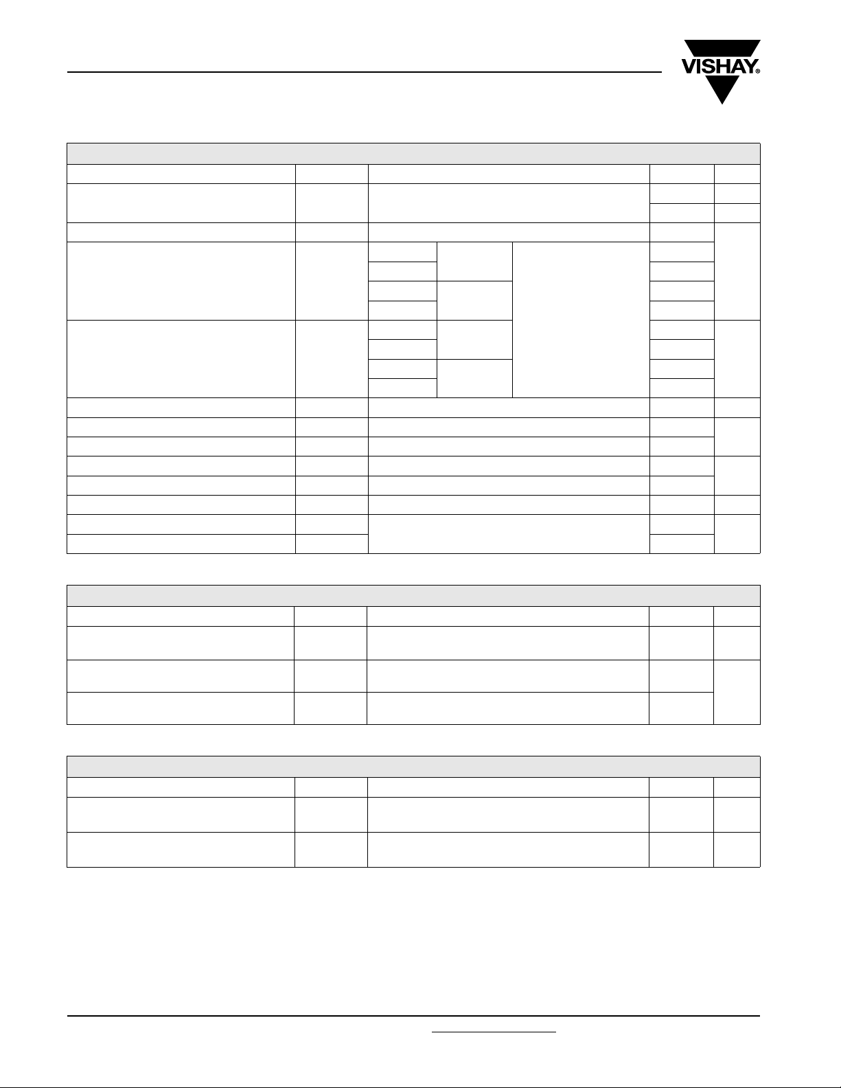
ABSOLUTE MAXIMUM RATINGS
PARAMETER SYMBOL TEST CONDITIONS VALUES UNITS
Maximum average on-state current
at case temperature
Maximum RMS on-state current I
I
T(RMS)
Maximum peak, one-cycle
non-repetitive surge current
2
Maximum I
Maximum I
t for fusing I2t
2
√t for fusing I2√t t = 0.1 to 10 ms, no voltage reapplied 1250 kA2√s
Low level value of threshold voltage V
High level value of threshold voltage V
Low level value of on-state slope resistance r
High level value of on-state slope resistance r
Maximum on-state voltage V
Maximum holding current I
Maximum (typical) latching current I
T(AV)
180° conduction, half sine wave
DC at 76 °C case temperature 314
I
TSM
T(TO)1
T(TO)2
t1
t2
TM
H
L
t = 10 ms
t = 8.3 ms 5230
t = 10 ms
t = 8.3 ms 4400
t = 10 ms
t = 8.3 ms 114
t = 10 ms
t = 8.3 ms 81
(16.7 % x π x I
(I > π x I
(16.7 % x π x I
(I > π x I
Ipk = 570 A, TJ = 125 °C, tp = 10 ms sine pulse 1.75 V
TJ = TJ maximum, anode supply 12 V resistive load
No voltage
reapplied
100 % V
reapplied
No voltage
RRM
Sinusoidal half wave,
initial T
= TJ maximum
J
reapplied
100 % V
RRM
reapplied
< I < π x I
T(AV)
), TJ = TJ maximum 1.14
T(AV)
< I < π x I
T(AV)
), TJ = TJ maximum 1.14
T(AV)
), TJ = TJ maximum 1.08
T(AV)
), TJ = TJ maximum 1.18
T(AV)
200 A
85 °C
5000
4200
125
88
600
1000 (300)
A
kA2s
V
mΩ
mA
SWITCHING
PARAMETER SYMBOL TEST CONDITIONS VALUES UNITS
Maximum non-repetitive rate of rise
of turned-on current
Typical delay time t
Typical turn-off time t
dI/dt
d
q
Gate drive 20 V, 20 Ω, t
T
= TJ maximum, anode voltage ≤ 80 % V
J
≤ 1 µs
r
DRM
Gate current 1 A, dIg/dt = 1 A/µs
V
= 0.67 % V
d
, TJ = 25 °C
DRM
ITM = 300 A, TJ = TJ maximum, dI/dt = 20 A/µs,
V
= 50 V, dV/dt = 20 V/µs, gate 0 V 100 Ω, tp = 500 µs
R
1000 A/µs
1.0
µs
100
BLOCKING
PARAMETER SYMBOL TEST CONDITIONS VALUES UNITS
Maximum critical rate of rise
of off-state voltage
Maximum peak reverse and
off-state leakage current
dV/dt T
,
I
RRM
I
DRM
= TJ maximum linear to 80 % rated V
J
TJ = TJ maximum, rated V
DRM/VRRM
DRM
500 V/µs
applied 30 mA
www.vishay.com For technical questions, contact: ind-modules@vishay.com
Document Number: 94397
2 Revision: 11-Aug-08

ST180SPbF Series
Phase Control Thyristors
Vishay High Power Products
(Stud Version), 200 A
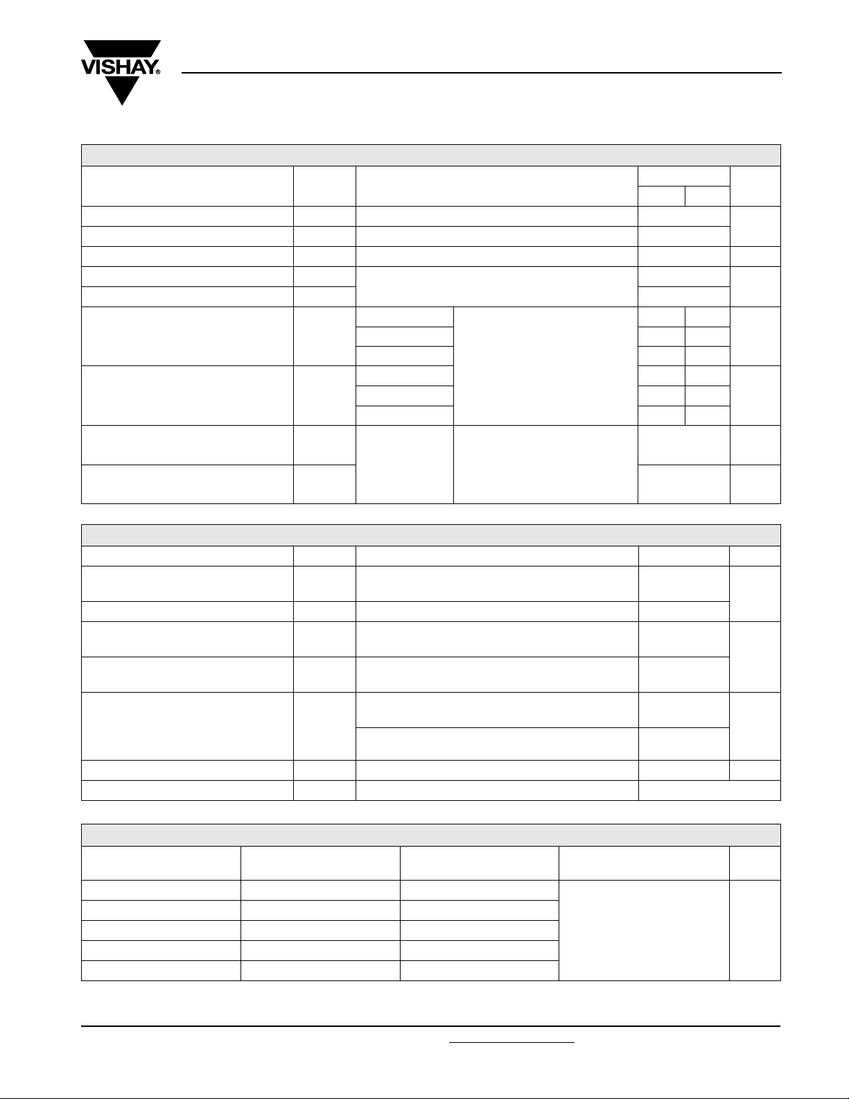
TRIGGERING
PARAMETER SYMBOL TEST CONDITIONS
Maximum peak gate power P
Maximum average gate power P
Maximum peak positive gate current I
Maximum peak positive gate voltage + V
Maximum peak negative gate voltage - V
GM
G(AV)
GM
TJ = TJ maximum, tp ≤ 5 ms 10
TJ = TJ maximum, f = 50 Hz, d% = 50 2.0
TJ = TJ maximum, tp ≤ 5 ms 3.0 A
GM
TJ = TJ maximum, tp ≤ 5 ms
GM
TJ = - 40 °C
DC gate current required to trigger I
DC gate voltage required to trigger V
DC gate current not to trigger I
DC gate voltage not to trigger V
GT
GT
GD
GD
= 25 °C 90 150
J
T
= 125 °C 40 -
J
TJ = - 40 °C 2.9 -
= 25 °C 1.8 3.0
T
J
T
= 125 °C 1.2 -
J
Maximum required gate trigger/
current/voltage are the lowest
value which will trigger all units
12 V anode to cathode applied
Maximum gate current/voltage
not to trigger is the maximum
TJ = TJ maximum
value which will not trigger any
unit with rated V
DRM
anode to
cathode applied
VALUES
TYP. MAX.
180 -
0.25 V
UNITS
20
5.0
mAT
10 mA
W
V
V
THERMAL AND MECHANICAL SPECIFICATIONS
PARAMETER SYMBOL TEST CONDITIONS VALUES UNITS
Maximum operating junction
temperature range
Maximum storage temperature range T
Maximum thermal resistance,
junction to case
Maximum thermal resistance,
case to heatsink
R
R
T
J
Stg
thJC
thC-hs
DC operation 0.105
Mounting surface, smooth, flat and greased 0.04
Non-lubricated threads
Mounting torque, ± 10 %
Lubricated threads
Approximate weight 280 g
Case style See dimensions - link at the end of datasheeet TO-209AB (TO-93)
ΔR
CONDUCTION
thJC
CONDUCTION ANGLE
SINUSOIDAL
CONDUCTION
RECTANGULAR
CONDUCTION
TEST CONDITIONS UNITS
180° 0.015 0.012
120° 0.019 0.020
T
90° 0.025 0.027
= TJ maximum K/W
J
60° 0.036 0.037
30° 0.060 0.060
Note
• The table above shows the increment of thermal resistance R
when devices operate at different conduction angles than DC
thJC
Document Number: 94397 For technical questions, contact: ind-modules@vishay.com
Revision: 11-Aug-08 3
- 40 to 125
- 40 to 150
31
(275)
24.5
(210)
°C
K/W
N · m
(lbf ⋅ in)
www.vishay.com
 Loading...