

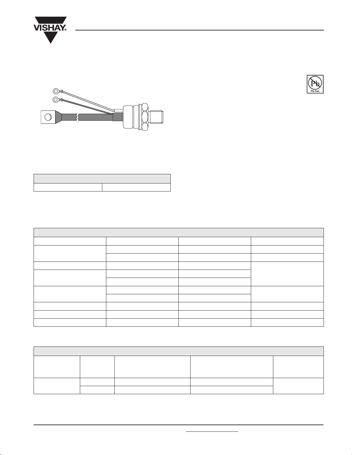
TO-209AB (TO-93)
Other voltage codes available.
Vishay High Power Products
Inverter Grade Thyristors
(Stud Version), 175 A
FEATURES
• All diffused design
• Center amplifying gate
• Guaranteed high dV/dt
• Guaranteed high dI/dt
• High surge current capability
• Low thermal impedance
• High speed performance
• Compression bonding
• Lead (Pb)-free
• Designed and qualified for industrial level
ST173SPbF Series
RoHS
COMPLIANT
PRODUCT SUMMARY
I
T(AV)
175 A
TYPICAL APPLICATIONS
•Inverters
• Choppers
• Induction heating
• All types of force-commutated converters
MAJOR RATINGS AND CHARACTERISTICS
PARAMETER TEST CONDITIONS VALUES UNITS
I
T(AV)
I
T(RMS)
I
TSM
2
I
t
V
DRM/VRRM
t
Range 15 to 25 µs
q
T
J
T
C
50 Hz 4680
60 Hz 4900
50 Hz 110
60 Hz 100
175 A
85 °C
275
1000 to 1200 V
- 40 to 125 °C
ELECTRICAL SPECIFICATIONS
A
kA2s
VOLTAGE RATINGS
TYPE NUMBER
ST173S
Document Number: 94367 For technical questions, contact: ind-modules@vishay.com
Revision: 29-Apr-08 1
V
VOLTAGE
CODE
10 1000 1100
12 1200 1300
DRM/VRRM
REPETITIVE PEAK VOLTAGE
, MAXIMUM
V
V
NON-REPETITIVE PEAK VOLTAGE
, MAXIMUM
RSM
I
DRM/IRRM
V
AT T
MAXIMUM
= TJ MAXIMUM
J
mA
40
www.vishay.com
ST173SPbF Series
Vishay High Power Products
Inverter Grade Thyristors
(Stud Version), 175 A
CURRENT CARRYING CAPABILITY
I
FREQUENCY UNITS
180° el
TM
180° el
50 Hz 500 320 790 550 4510 3310
400 Hz 450 290 810 540 1970 1350
1000 Hz 330 190 760 490 1050 680
2500 Hz 170 80 510 300 480 280
Recovery voltage V
r
Voltage before turn-on V
d
50 50 50
V
DRM
V
Rise of on-state current dI/dt 50 - - A/µs
Case temperature 60 85 60 85 60 85 °C
Equivalent values for RC circuit 47/0.22 47/0.22 47/0.22 Ω/µF
ON-STATE CONDUCTION
PARAMETER SYMBOL TEST CONDITIONS VALUES UNITS
Maximum average on-state current
at case temperature
Maximum RMS on-state current I
Maximum peak, one half cycle,
non-repetitive surge current
2
Maximum I
Maximum I
t for fusing I2t
2
√t for fusing I2√t t = 0.1 to 10 ms, no voltage reapplied 1100 kA2√s
Maximum peak on-state voltage V
Low level value of threshold voltage V
High level value of threshold voltage V
Low level value of forward slope resistance r
High level value of forward slope resistance r
Maximum holding current I
Typical latching current I
I
T(AV)
T(RMS)
I
TSM
TM
T(TO)1
T(TO)2
t1
t2
H
L
180° conduction, half sine wave
DC at 75 °C case temperature 275
t = 10 ms
t = 8.3 ms 4900
t = 10 ms
t = 8.3 ms 4120
t = 10 ms
t = 8.3 ms 100
t = 10 ms
t = 8.3 ms 71
No voltage
reapplied
100 % V
reapplied
No voltage
reapplied
100 % V
reapplied
ITM = 600 A, TJ = TJ maximum,
= 10 ms sine wave pulse
t
p
(16.7 % x π x I
(I > π x I
T(AV)
(16.7 % x π x I
(I > π x I
T(AV)
< I < π x I
T(AV)
), TJ = TJ maximum 1.58
< I < π x I
T(AV)
), TJ = TJ maximum 0.82
TJ = 25 °C, IT > 30 A 600
TJ = 25 °C, VA = 12 V, Ra = 6 Ω, IG = 1 A 1000
DRM
I
TM
RRM
Sinusoidal half wave,
initial T
RRM
), TJ = TJ maximum 1.55
T(AV)
), TJ = TJ maximum 0.87
T(AV)
100 µs
V
= TJ maximum
J
DRM
I
TM
175 A
85 °C
4680
3940
110
77
2.07
A
V
A
kA2s
V
mΩ
mA
SWITCHING
PARAMETER SYMBOL TEST CONDITIONS VALUES UNITS
Maximum non-repetitive rate of rise
of turned on current
Typical delay time t
dI/dt
d
minimum
Maximum turn-off time
maximum 25
t
q
www.vishay.com For technical questions, contact: ind-modules@vishay.com
2 Revision: 29-Apr-08
= TJ maximum, V
T
J
= Rated V
DRM
DRM
ITM = 2 x dI/dt
TJ = 25 °C, VDM = Rated V
, ITM = 50 A DC, tp = 1 µs
DRM
Resistive load, gate pulse: 10 V, 5 Ω source
TJ = TJ maximum,
I
= 300 A, commutating dI/dt = 20 A/µs
TM
= 50 V, tp = 500 µs, dV/dt: See table in device code
V
R
1000 A/µs
1.1
15
µs
Document Number: 94367
ST173SPbF Series
Inverter Grade Thyristors
Vishay High Power Products
(Stud Version), 175 A
BLOCKING
PARAMETER SYMBOL TEST CONDITIONS VALUES UNITS
= TJ maximum, linear to 80 % V
T
Maximum critical rate of rise of off-state voltage dV/dt
I
Maximum peak reverse and off-state leakage current
RRM
I
DRM
J
higher value available on request
,
TJ = TJ maximum, rated V
DRM/VRRM
TRIGGERING
PARAMETER SYMBOL TEST CONDITIONS VALUES UNITS
Maximum peak gate power P
Maximum average gate power P
Maximum peak positive gate current I
Maximum peak positive gate voltage + V
Maximum peak negative gate voltage - V
Maximum DC gate currrent required to trigger I
Maximum DC gate voltage required to trigger V
Maximum DC gate current not to trigger I
Maximum DC gate voltage not to trigger V
GM
G(AV)
GM
GM
GM
GT
GT
GD
GD
TJ = TJ maximum, f = 50 Hz, d% = 50
TJ = TJ maximum, tp ≤ 5 ms
TJ = 25 °C, VA = 12 V, Ra = 6 Ω
TJ = TJ maximum, rated V
DRM
applied
,
DRM
500 V/µs
applied 40 mA
60
10
10 A
20
5
200 mA
3V
20 mA
0.25 V
W
V
THERMAL AND MECHANICAL SPECIFICATIONS
PARAMETER SYMBOL TEST CONDITIONS VALUES UNITS
Maximum junction operating temperature range T
Maximum storage temperature range T
Maximum thermal resistance, junction to case R
Maximum thermal resistance, case to heatsink R
Stg
thJC
thCS
J
DC operation 0.105
Mounting surface, smooth, flat and greased 0.04
Non-lubricated threads
Mounting torque, ± 10 %
Lubricated threads
Approximate weight 280 g
Case style See dimensions - link at the end of datasheet TO-209AB (TO-93)
ΔR
CONDUCTION
thJC
CONDUCTION ANGLE
SINUSOIDAL
CONDUCTION
RECTANGULAR
CONDUCTION
TEST CONDITIONS UNITS
180° 0.016 0.012
120° 0.019 0.020
T
90° 0.025 0.027
= TJ maximum K/W
J
60° 0.036 0.037
30° 0.060 0.060
Note
• The table above shows the increment of thermal resistance R
when devices operate at different conduction angles than DC
thJC
- 40 to 125
- 40 to 150
31
(275)
24.5
(210)
(lbf · in)
°C
K/W
N · m
Document Number: 94367 For technical questions, contact: ind-modules@vishay.com
www.vishay.com
Revision: 29-Apr-08 3
ST173SPbF Series
Vishay High Power Products
130
120
110
100
Maximum Allowable
90
Case Temperature (°C)
80
350
300
250
200
150
Power Loss (W)
100
50
Maximum Average On-State
30 °C
0
40 80 120 160
20 60 100 140 180
Average On-State Current (A)
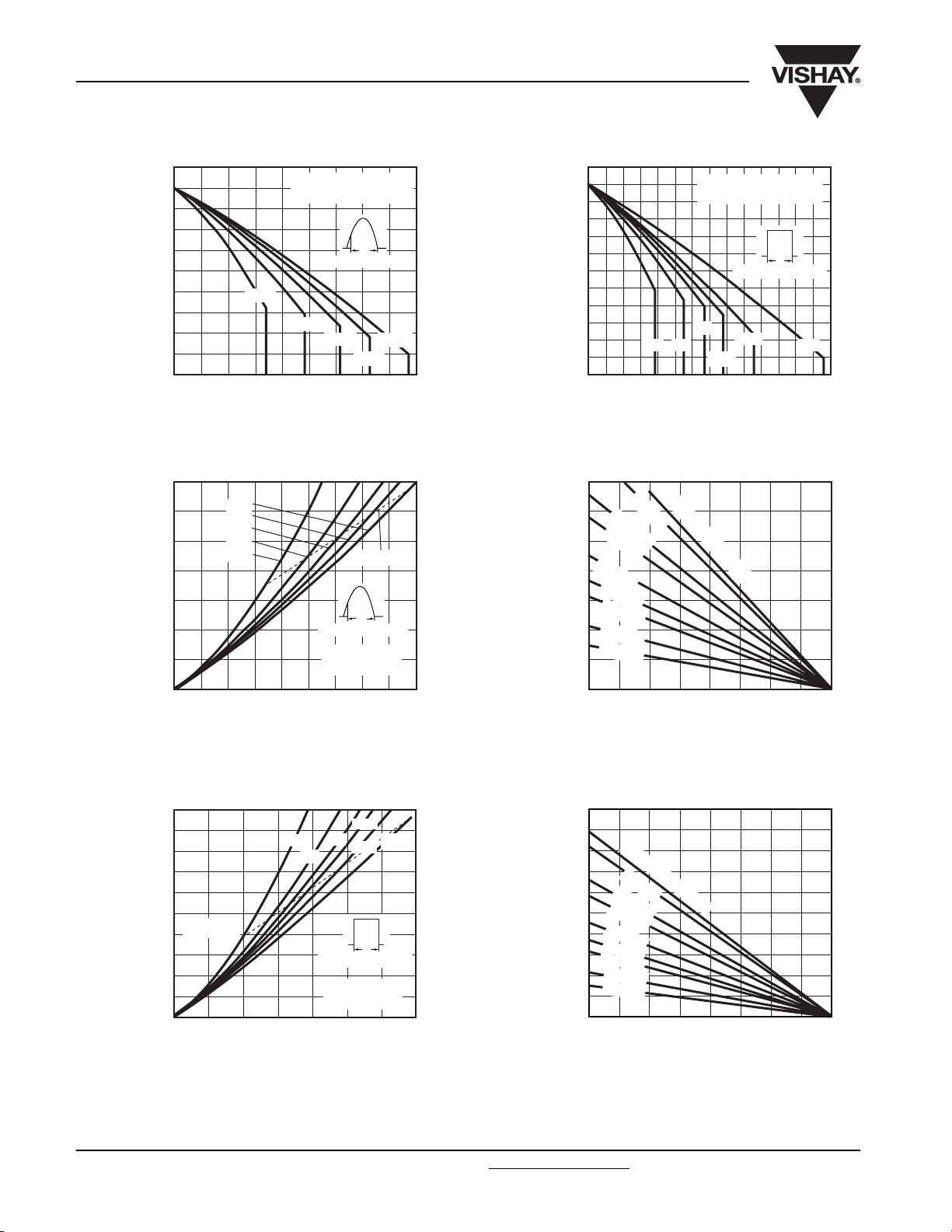
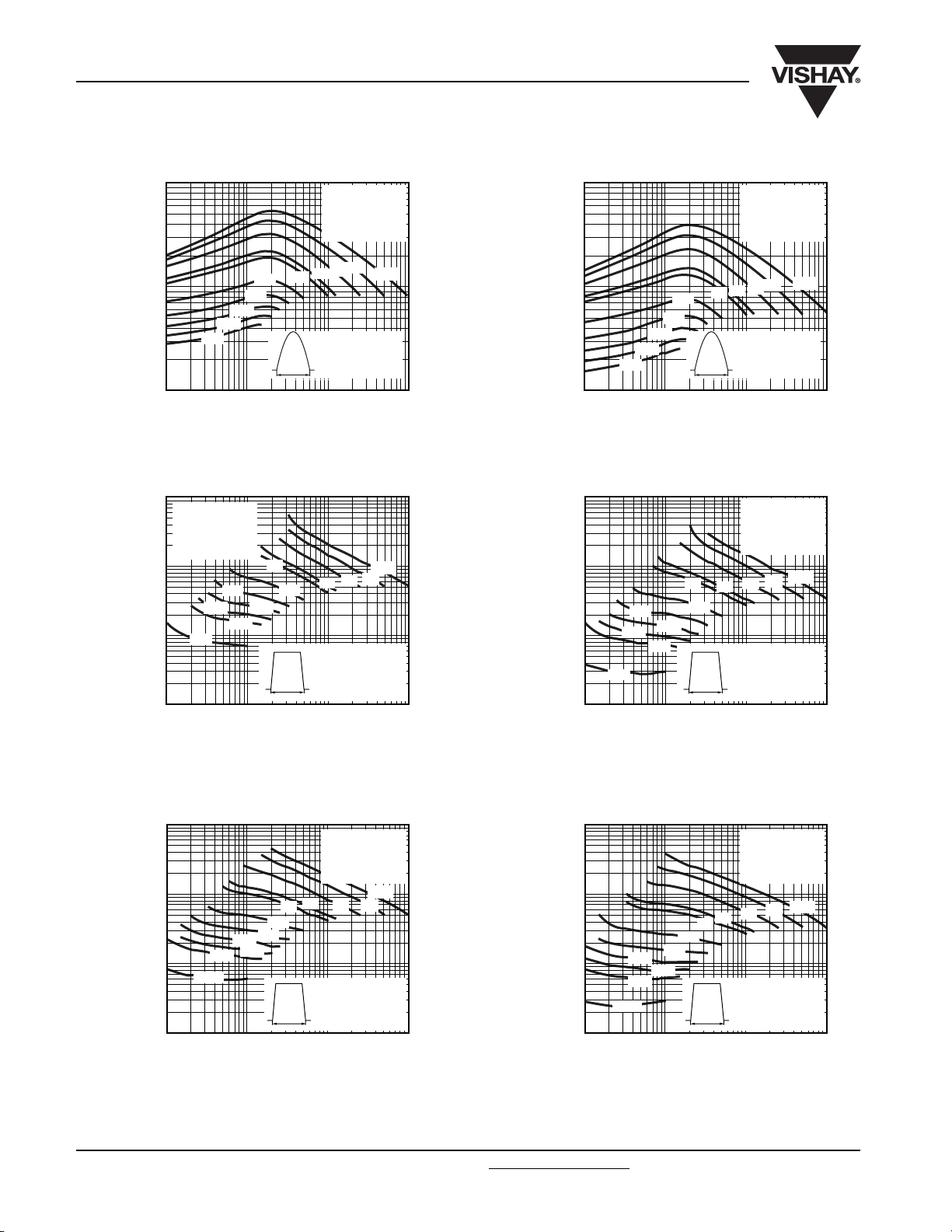
Fig. 1 - Current Ratings Characteristics Fig. 2 - Current Ratings Characteristics
180°
120°
90°
60°
30°
0
20 6040 80
0
Average On-State Current (A)
ST173S Series
(DC) = 0.105 K/W
R
thJC
Conduction angle
60 °C
90 °C 180 °C
Conduction angle
ST173S Series
= 125 °C
T
J
100 120 140 160 180
Inverter Grade Thyristors
(Stud Version), 175 A
130
120
Ø
120 °C
RMS limit
Ø
Fig. 3 - On-State Power Loss Characteristics
110
100
90
Maximum Allowable
Case Temperature (°C)
80
70
350
300
250
200
150
Power Loss (W)
100
50
Maximum Average On-State
Maximum Allowable Ambient Temperature (°C)
0
0
0.3 K/W
1.2 K/W
25
ST173S Series
(DC) = 0.105 K/W
R
thJC
Conduction period
90°
30° 60°
80 160
40 120
180°
120°
Average On-State Current (A)
0.1 K/W
R
0.16 K/W
0.2 K/W
0.4 K/W
0.5 K/W
0.8 K/W
thSA
= 0.08 K/W - ΔR
50 10075
Ø
DC
200 240 280
125
500
400
300
200
Maximum Average
100
On-State Power Loss (W)
0
RMS limit
0
120°
90°
80 160
40 120
30°
60°
180°
Conduction period
ST173S Series
= 125 °C
T
J
200 240 280
Average On-State Current (A)
DC
Ø
500
400
300
200
Power Loss (W)
100
Maximum Average On-State
0
R
thSA
= 0.8 K/W - ΔR
0.1 K/W
0.16 K/W
0.2 K/W
0.3 K/W
0.4 K/W
0.5 K/W
0.8 K/W
1.2 K/W
25 50 75 100 125
Maximum Allowable Ambient Temperature (°C)
Fig. 4 - On-State Power Loss Characteristics
www.vishay.com For technical questions, contact: ind-modules@vishay.com
Document Number: 94367
4 Revision: 29-Apr-08

ST173SPbF Series
4500
4000
3500
3000
On-State Current (A)
Peak Half Sine Wave
2500
2000
At any rated load condition and with
rated V
ST173S Series
1 10 100
Number of Equal Amplitude Half Cycle
Fig. 5 - Maximum Non-Repetitive Surge Current
5000
4500
4000
3500
3000
2500
On-State Current (A)
Peak Half Sine Wave
2000
1500
ST173S Series
0.01 0.1 1
Fig. 6 - Maximum Non-Repetitive Surge Current
Inverter Grade Thyristors
(Stud Version), 175 A
applied following surge.
RRM
Current Pulses (N)
Maximum non-repetitive surge current
versus pulse train duration. Control
of conduction may not be maintained.
Pulse Train Duration (s)
Initial TJ = 125 °C
at 60 Hz 0.0083 s
at 50 Hz 0.0100 s
Initial TJ = 125 °C
No voltage reapplied
Rated V
RRM
reapplied
Vishay High Power Products
1
Steady state value
= 0.105 K/W
R
thJC
(DC operation)
0.1
(K/W)
thJC
0.01
Transient Thermal
Impedance Z
0.001
0.01 0.1 1 100.001
Square Wave Pulse Duration (s)
Fig. 8 - Thermal Impedance Z
250
ST173S Series
= 125 °C
T
200
150
100
- Maximum Reverse
rr
Recovery Charge (µC)
Q
J
50
0
200 406080100
dI/dt - Rate of Fall of On-State Current (A/µs)
Fig. 9 - Reverse Recovered Current Characteristics
ST173S Series
Characteristics
thJC
I
TM
I
I
TM
= 100 A
I
TM
ITM = 50 A
= 500 A
= 300 A
TM
= 200 A
10 000
ST173S Series
1000
Instantaneous On-State Current (A)
100
1.0 1.5 2.0 2.5 3.0 3.5 4.0 4.5
Instantaneous On-State Voltage (V)
Fig. 7 - On-State Voltage Drop Characteristics
TJ = 125 °C
TJ = 25 °C
160
140
120
100
80
60
- Maximum Reverse
40
rr
Recovery Current (A)
I
20
0
I
TM = 500 A
I
TM = 300 A
I
TM = 200 A
I
TM = 100 A
I
TM = 50 A
ST173S Series
T
= 125 °C
J
200 40 60 80 100
dI/dt - Rate of Fall of On-State Current (A/µs)
Fig. 10 - Reverse Recovery Current Characteristics
Document Number: 94367 For technical questions, contact: ind-modules@vishay.com
www.vishay.com
Revision: 29-Apr-08 5
ST173SPbF Series
Vishay High Power Products
10 000
1000
3000
1000
1500
2000
2500
Peak On-State Current (A)
100
10 100 1000 10 000
Pulse Basewidth (µs)
10 000
1000
100
Snubber circuit
= 47 Ω
R
s
= 0.22 µF
C
s
= 80 % V
V
D
5000
DRM
1500
2500
3000
500
1000
2000
Peak On-State Current (A)
10
10 100 1000 10 000
Pulse Basewidth (µs)
400
500
ST173S Series
Sinusoidal pulse
t
T
p
400
ST173S Series
Trapezoidal pulse
T
C
t
p
dI/dt = 50 A/µs
Snubber circuit
= 47 Ω
R
s
= 0.22 µF
C
s
V
D
200
= 60 °C
C
= 60 °C
Inverter Grade Thyristors
(Stud Version), 175 A
= 80 % V
200
100
DRM
50 Hz
Fig. 11 - Frequency Characteristics
50 Hz
100
Fig. 12 - Frequency Characteristics
10 000
1000
Peak On-State Current (A)
3000
1000
1500
2000
2500
100
10 100 1000 10 000
Pulse Basewidth (µs)
10 000
1000
1500
2000
100
Peak On-State Current (A)
10
2500
3000
5000
10 100 1000 10 000
Pulse Basewidth (µs)
500
1000
500
t
p
400
t
p
Snubber circuit
= 47 Ω
R
s
= 0.22 µF
C
s
= 80 % V
V
D
50 Hz
100
200
400
ST173S Series
Sinusoidal pulse
= 85 °C
T
C
Snubber circuit
= 47 Ω
R
s
= 0.22 µF
C
s
= 80 % V
V
D
50 Hz
100
200
ST173S Series
Trapezoidal pulse
= 85 °C
T
C
dI/dt = 50 A/µs
DRM
DRM
10 000
1000
2000
2500
100
5000
10 000
Peak On-State Current (A)
10
10 100 1000 10 000
Pulse Basewidth (µs)
1500
1000
500
400
t
p
Snubber circuit
= 47 Ω
R
s
= 0.22 µF
C
s
= 80 % V
V
D
200
DRM
50 Hz
100
ST173S Series
Trapezoidal pulse
= 60 °C
T
C
dI/dt = 100 A/µs
10 000
1000
1500
5000
10 000
2000
2500
100
Peak On-State Current (A)
10
10 100 1000 10 000
Pulse Basewidth (µs)
1000
500
400
t
p
Snubber circuit
= 47 Ω
R
s
= 0.22 µF
C
s
= 80 % V
V
D
200
100
DRM
50 Hz
ST173S Series
Trapezoidal pulse
= 85 °C
T
C
dI/dt = 100 A/µs
Fig. 13 - Frequency Characteristics
www.vishay.com For technical questions, contact: ind-modules@vishay.com
Document Number: 94367
6 Revision: 29-Apr-08

ST173SPbF Series
100 000
10 000
1000
100
Peak On-State Current (A)
t
10
p
10 100 1000 10 000
1
0.5
0.3
0.2
0.1
ST173S Series
Sinusoidal pulse
Pulse Basewidth (µs)
100
Rectangular gate pulse
a) Recommended load line for
rated dI/dt: 20 V, 10 Ω; t
b) Recommended load line for
≤ 30 % rated dI/dt: 10 V, 10 Ω
10
≤ 1 µs
t
r
1
Instantaneous Gate Voltage (V)
0.1
0.001
4
2
Inverter Grade Thyristors
Vishay High Power Products
(Stud Version), 175 A
100 000
20 joules per pulse
7.5
10 000
1000
100
Peak On-State Current (A)
10
10 100 1000 10 000
Fig. 14 - Maximum On-State Energy Power Loss Characteristics
≤ 1 µs
r
(a)
(b)
T
J
T
J
= 25 °C
= 40 °C
Frequency limited by P
T
J
= 125 °C
V
GD
I
GD
Device: ST173S Series
0.01 0.1 1 10 100
Instantaneous Gate Current (A)
Fig. 15 - Gate Characteristics
ST173S Series
Rectangular pulse
t
dI/dt = 50 A/µs
p
0.5
0.4
0.3
0.2
0.1
Pulse Basewidth (µs)
(1) PGM = 10 W, tp = 20 ms
= 20 W, tp = 10 ms
(2) P
GM
(3) P
= 40 W, tp = 5 ms
GM
(4) P
= 60 W, tp = 3.3 ms
GM
(1) (2)
G(AV)
1
20 joules per pulse
5
3
2
(3)
(4)
10
Document Number: 94367 For technical questions, contact: ind-modules@vishay.com
www.vishay.com
Revision: 29-Apr-08 7

ST173SPbF Series
Vishay High Power Products
ORDERING INFORMATION TABLE
Device code
ST 17 3 S 12 P F K 0 - PbF
324
1 - Thyristor
2 - Essential part number
3 - 3 = Fast turn-off
4 - S = Compression bonding stud
5 - Voltage code x 100 = V
6 - P = Stud base 3/4" 16UNF-2A
M = Stud base metric threads M16 x 1.5
7 - Reapplied dV/dt code (for t
8 -t
9 - 0 = Eyelet terminals
10
11
code
q
(gate and aux. cathode leads)
1 = Fast-on terminals
(gate and aux. cathode leads)
2 = Flag terminals (for cathode and gate terminals)
- Critical dV/dt:
None = 500 V/µs (standard value)
L = 1000 V/µs (special selection)
- Lead (Pb)-free
Inverter Grade Thyristors
(Stud Version), 175 A
51
6 7 8 9 10 11
(see Voltage Ratings table)
RRM
test condition)
q
t
* Standard part number.
All other types available only on request.
dV/dt - tq combinations available
dV/dt (V/µs) 20 50 100 200 400
---
CL
CP
CK
CJ
DP
EP
DK
EK
DJ
EJ
DH
-
EH
q
(µs)
15
18
20
25
30
FP*
FK*
HK
HJ
FHFJHH
-
-
LINKS TO RELATED DOCUMENTS
Dimensions http://www.vishay.com/doc?95079
www.vishay.com For technical questions, contact: ind-modules@vishay.com
8 Revision: 29-Apr-08
Document Number: 94367
Fast-on Terminals
AMP. 280000-1
REF-250
90 (3.54) MIN.
19 (0.75) MAX.
4 (0.16) MAX.
White gate
Red shrink
Red cathode
Red silicon rubber
210 (8.26) ± 10 (0.39)
C.S. 0.4 mm
2
(0.006 s.i.)
4.3 (0.17) DIA.
38.5 (1.52)
MAX.
16 (0.63) MAX.
8.5 (0.33) DIA.
27.5 (1.08)
MAX. DIA.
220 (8.66) ± 10 (0.39)
SW 32
C.S. 25 mm
2
(0.039 s.i.)
Flexible leads
22 (0.86) MIN.
35 (1.38)
MAX.
3/4"-16UNF-2A
(1)
27.5 (1.08)
MAX.
White shrink
9.5 (0.37) MIN.
Ceramic housing
TO-209AB (TO-93)
DIMENSIONS - TO-209AB (TO-93) in millimeters (inches)
Outline Dimensions
Vishay Semiconductors
Note
(1)
For metric device: M16 x 1.5 - length 21 (0.83) maximum
Document Number: 95079 For technical questions, contact: indmodules@vishay.com
Revision: 01-Aug-07 1
www.vishay.com

Outline Dimensions
Vishay Semiconductors
TO-209AB (TO-93)
DIMENSIONS - TO-209AB (TO-93) FLAG TERMINALS in millimeters (inches)
Ceramic housing
80 (3.15) MAX.
27.5 (1.08) MAX. 38.5 (1.52) MAX.
1.5 (0.06) DIA.
DIA. 27.5 (1.08) MAX.
16 (0.63)
MAX.
SW 32
22 (0.89)
14 (0.55)
DIA. 6.5 (0.25)
13 (0.51)
3/4"-16UNF-2A
Note
(2)
For metric device: M16 x 1.5 - length 21 (0.83) maximum
(1)
3 (0.12)
www.vishay.com For technical questions, contact: indmodules@vishay.com
2 Revision: 01-Aug-07
Document Number: 95079

Legal Disclaimer Notice
www.vishay.com
Vishay
Disclaimer
ALL PRODUCT, PRODUCT SPECIFICATIONS AND DATA ARE SUBJECT TO CHANGE WITHOUT NOTICE TO IMPROVE
RELIABILITY, FUNCTION OR DESIGN OR OTHERWISE.
Vishay Intertechnology, Inc., its affiliates, agents, and employees, and all persons acting on its or their behalf (collectively,
“Vishay”), disclaim any and all liability for any errors, inaccuracies or incompleteness contained in any datasheet or in any other
disclosure relating to any product.
Vishay makes no warranty, representation or guarantee regarding the suitability of the products for any particular purpose or
the continuing production of any product. To the maximum extent permitted by applicable law, Vishay disclaims (i) any and all
liability arising out of the application or use of any product, (ii) any and all liability, including without limitation special,
consequential or incidental damages, and (iii) any and all implied warranties, including warranties of fitness for particular
purpose, non-infringement and merchantability.
Statements regarding the suitability of products for certain types of applications are based on Vishay’s knowledge of typical
requirements that are often placed on Vishay products in generic applications. Such statements are not binding statements
about the suitability of products for a particular application. It is the customer’s responsibility to validate that a particular
product with the properties described in the product specification is suitable for use in a particular application. Parameters
provided in datasheets and/or specifications may vary in different applications and performance may vary over time. All
operating parameters, including typical parameters, must be validated for each customer application by the customer’s
technical experts. Product specifications do not expand or otherwise modify Vishay’s terms and conditions of purchase,
including but not limited to the warranty expressed therein.
Except as expressly indicated in writing, Vishay products are not designed for use in medical, life-saving, or life-sustaining
applications or for any other application in which the failure of the Vishay product could result in personal injury or death.
Customers using or selling Vishay products not expressly indicated for use in such applications do so at their own risk and agree
to fully indemnify and hold Vishay and its distributors harmless from and against any and all claims, liabilities, expenses and
damages arising or resulting in connection with such use or sale, including attorneys fees, even if such claim alleges that Vishay
or its distributor was negligent regarding the design or manufacture of the part. Please contact authorized Vishay personnel to
obtain written terms and conditions regarding products designed for such applications.
No license, express or implied, by estoppel or otherwise, to any intellectual property rights is granted by this document or by
any conduct of Vishay. Product names and markings noted herein may be trademarks of their respective owners.
Material Category Policy
Vishay Intertechnology, Inc. hereby certifies that all its products that are identified as RoHS-Compliant fulfill the
definitions and restrictions defined under Directive 2011/65/EU of The European Parliament and of the Council
of June 8, 2011 on the restriction of the use of certain hazardous substances in electrical and electronic equipment
(EEE) - recast, unless otherwise specified as non-compliant.
Please note that some Vishay documentation may still make reference to RoHS Directive 2002/95/EC. We confirm that
all the products identified as being compliant to Directive 2002/95/EC conform to Directive 2011/65/EU.
Revision: 12-Mar-12
1
Document Number: 91000
 Loading...