

SST200/200A
Vishay Siliconix
N-Channel JFETs
PRODUCT SUMMARY
V
(V) V
GS(off)
-0.3 to - 0.9 -25 0.25 0.15
FEATURES BENEFITS APPLICATIONS
D Low Cutoff Voltage: <0.9 V
D High Input Impedance
D Very Low Noise
D High Gain: A
V
Min (V) gfS Min (mS) I
(BR)GSS
= 80 @ 20 mA
Min (mA)
DSS
D High Quality Low-Level Signal
Amplification
D Low Signal Loss/System Error
D High System Sensitivity
D Mini-Microphones
D Hearing Aids
D High-Gain, Low-Noise Amplifiers
D Low-Current, Low-Voltage
Battery-Powered Amplifiers
D Ultra High Input Impedance
Pre-Amplifiers
DESCRIPTION
The SST200/200A features low leakage, very low noise and
low cutoff voltage for use with low-level power supplies. The
SST200/200A is excellent for battery powered equipment and
low current amplifiers such as mini-microphones.
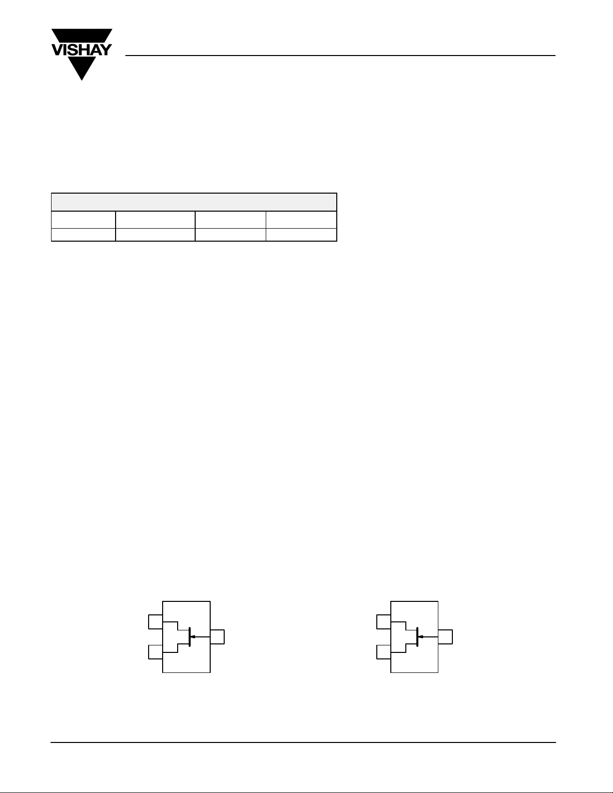
TO-236
(SOT-23)
D
1
G
3
S
2
Top View
SST200 (S2)*
*Marking Code for TO-236
The TO-236 (SOT-23) and SOT-323 (SC-70 3-leads)
packages, provide surface-mount capability and is available in
tape-and-reel for automated assembly.
For applications information see AN102 and AN106.
SOT-323
(SC-70 3-LEADS)
1
D
3
SG2
Top View
SST200A (C)*
*Marking Code for SOT-323
Document Number: 70976
S-31623—Rev. E, 01-Sep-03
www.vishay.com
1
SST200/200A
V
VDS = 15 V, VGS = 0 V
Vishay Siliconix
ABSOLUTE MAXIMUM RATINGS
Gate-Drain, Gate-Source Voltage -25 V. . . . . . . . . . . . . . . . . . . . . . . . . . . . . . .
Gate Current 10 mA. . . . . . . . . . . . . . . . . . . . . . . . . . . . . . . . . . . . . . . . . . . . . . . . .
Lead Temperature (1/16” from case for 10 sec.) 300_C. . . . . . . . . . . . . . . . . . .
Storage Temperature -55 to 150_C. . . . . . . . . . . . . . . . . . . . . . . . . . . . . . . . . . .
Operating Junction Temperature -55 to 150_C. . . . . . . . . . . . . . . . . . . . . . . . .
Power Dissipation
To-236 (SOT-23)
b
SC-70
Notes
a. Derate 2.8 mW/_C above 25_C
b. Derate 1.2 mW/_C above 25_C
SPECIFICATIONS (TA = 25_C UNLESS OTHERWISE NOTED)
Parameter Symbol Test Conditions Min Typ
Static
Gate-Source
Breakdown Voltage
Gate-Source Cutoff Voltage V
Saturation Drain Current
Gate Reverse Current I
Gate Operating Current I
Drain Cutoff Current I
Gate-Source Forward Voltage V
b
Dynamic
Common-Source
Forward Transconductance
Common-Source
Input Capacitance
Common-Source
Reverse Transfer Capacitance
Equivalent Input Noise Voltage e
V
(BR)GSS
GS(off)
I
DSS
GSS
D(off)
GS(F)
g
C
C
IG = -1 mA , VDS = 0 V
VDS = 15 V, ID = 1.0 mA
VDS = 15 V, VGS = 0 V 0.15 0.7 mA
VGS = -20 V, VDS = 0 V -2 -100 pA
TA = 125_C
G
fs
iss
rss
n
VDG = 10 V, ID = 0.1 mA -2
VDS = 15 V, VGS = -5 V 2
IG = 1 mA , VDS = 0 V 0.7 V
VDS = 15 V, VGS = 0 V
f = 1 kHz
VDS = 15 V, VGS = 0 V
f = 1 MHz
VDS = 10 V, VGS = 0 V
f = 1 kHz
a
350 mW. . . . . . . . . . . . . . . . . . . . . . . . . . . . . . . . . . . . . . . . . .
150 mW. . . . . . . . . . . . . . . . . . . . . . . . . . . . . . . . . . . . . . . . . . . . . . . . . . .
Limits
a
Max Unit
-25
-0.3 -0.9
-1 nA
0.25 0.7 mS
4.5
1.3
6
V
pA
pF
nV⁄
√Hz
Notes
a. Typical values are for DESIGN AID ONLY, not guaranteed nor subject to production testing. NPA
b. Pulse test: PW v300 ms duty cycle v3%.
www.vishay.com
2
Document Number: 70976
S-31623—Rev. E, 01-Sep-03

TYPICAL CHARACTERISTICS (TA = 25_C UNLESS OTHERWISE NOTED)
Drain Current and Transconductance
1.0
vs. Gate-Source Cutoff Voltage
I
0.9
0.8
@ VDS = 10 V, VGS = 0 V
g
fs
f = 1 kHz
@ VDS = 10 V, V
DSS
0.7
0.6
0.5
0.4
0.3
0.2
- Saturation Drain Current (mA)
DSS
0.1
I
0.0
0.0 0.2 0.4 0.6 0.8 1.0
V
- Gate-Source Cutoff Voltage (V)
GS(off)
= 0 V
GS
g
fs
I
DSS
2.0
1.8
1.6
1.4
1.2
1.0
0.8
0.6
0.4
0.2
0
10 nA
g
fs
- Forward Transconductance (µS)
1 nA
100 pA
10 pA
- Gate Leakage
G
I
TA = 25_C
1 pA
0.1 pA
01530
Gate Leakage Current
TA = 125_C
V
- Drain-Gate Voltage (V)
DG
SST200/200A
Vishay Siliconix
IG @ ID = 500 mA
ID = 100 mA
I
@ 125_C
GSS
ID = 500 mA
ID = 100 mA
I
@ 25_C
GSS
400
V
= -0.7 V
GS(off)
VGS = 0 V
360
240
160
- Drain Current (mA)
D
I
80
-0.5 V
-0.1 V
-0.2 V
-0.3 V
-0.4 V
0
01216420
8
VDS - Drain-Source Voltage (V)
Transconductance vs. Gate-Source Voltage
1.5
V
= -0.7 V
GS(off)
1.2
TA = -55_C
Output Characteristics
0.9
25_C
- Drain Current (mA)
D
I
500
Transfer Characteristics
= -0.7 V
GS(off)
400
300
TA = -55_C
25_C
200
125_C
100
0
0 -0.3-0.2-0.1 -0.4 -0.5
VGS - Gate-Source Voltage (V)
VDS = 10 V
f = 1 kHz
VDS = 10 VV
Document Number: 70976
S-31623—Rev. E, 01-Sep-03
0.6
125_C
0.3
- Forward Transconductance (mS)
fs
g
0
0 - 0.3 -0.4- 0.2-0.1 -0.5
- Gate-Source Voltage (V)
V
GS
www.vishay.com
3

SST200/200A
Vishay Siliconix
TYPICAL CHARACTERISTICS (TA = 25_C UNLESS OTHERWISE NOTED)
- Voltage Gain
V
A
- Input Capacitance (pF)C
iss
200
160
120
80
40
0
10
8
6
4
2
0
0 -12 -16 -20-8-4
Circuit Voltage Gain vs. Drain Current
g
AV+
Assume VDD = 15 V, VDS = 5 V
R
L
fsRL
1 ) RLg
10 V
+
I
D
-1.5 V
I
- Drain Current (mA)
D
os
V
= -0.7 V
GS(off)
0.1 10.01 0.01 0.1 1
Common-Source Input Capacitance
vs. Gate-Source Voltage
f = 1 MHz
VDS = 0 V
10 V
V
- Gate-Source Voltage (V)
GS
On-Resistance vs. Drain Current
V
= -0.7 V
GS(off)
-1.5 V
ID - Drain Current (mA)
- Drain-Source On-Resistance ( Ω )
r
2000
1600
1200
800
400
DS(on)
0
Common-Source Reverse Feedback Capacitance
5
4
3
2
1
- Reverse Feedback Capacitance (pF)
rss
C
0
0 -12 -20-16-8-4
vs. Gate-Source Voltage
f = 1 MHz
VDS = 0 V
10 V
VGS - Gate-Source Voltage (V)
Equivalent Input Noise Voltage vs. Frequency
20
16
12
8
en - Noise Voltage nV / Hz
4
0
10 100 1 k 100 k10 k
www.vishay.com
4
VDS = 10 V
V
GS
ID @ 100 mA
= 0 V
f - Frequency (Hz)
300
240
180
120
- Drain Current (µA)
D
I
60
0
0 0.5
Output Characteristics
V
= -0.7 V
GS(off)
-0.5
0.1 0.2 0.3 0.4
V
- Drain-Source Voltage (V)
DS
Document Number: 70976
S-31623—Rev. E, 01-Sep-03
VGS = 0 V
-0.1
-0.2
-0.3
-0.4

 Loading...