

www.vishay.com
S
G
D
P-Channel MOSFET
G
TO-236
(SOT-23)
S
D
Top View
SQ2309ES*
* Marking Code:8Pxxx
2
3
1
Automotive P-Channel 60 V (D-S) 175 °C MOSFET
PRODUCT SUMMARY
VDS (V) - 60
() at VGS = - 10 V 0.335
R
DS(on)
R
() at VGS = - 4.5 V 0.500
DS(on)
(A) - 1.7
I
D
Configuration Single
Vishay Siliconix
FEATURES
• Halogen-free According to IEC 61249-2-21
Definition
®
•TrenchFET
• AEC-Q101 Qualified
•100 % Rg and UIS Tested
• Compliant to RoHS Directive 2002/95/EC
Power MOSFET
c
SQ2309ES
ORDERING INFORMATION
Package SOT-23
Lead (Pb)-free and Halogen-free SQ2309ES-T1-GE3
ABSOLUTE MAXIMUM RATINGS (TC = 25 °C, unless otherwise noted)
PARAMETER SYMBOL LIMIT UNIT
Drain-Source Voltage V
Gate-Source Voltage V
= 25 °C
T
Continuous Drain Current
C
T
= 125 °C - 1
C
Continuous Source Current (Diode Conduction) I
Pulsed Drain Current
Single Pulse Avalanche Current
Single Pulse Avalanche Energy E
Maximum Power Dissipation
a
L = 0.1 mH
a
TC = 25 °C
T
= 125 °C 0.6
C
Operating Junction and Storage Temperature Range T
DS
± 20
GS
I
D
S
IDM - 6.8
I
AS
AS
P
D
, T
J
stg
- 60
V
- 1.7
- 2.6
A
- 15
11 mJ
2
W
- 55 to + 175 °C
THERMAL RESISTANCE RATINGS
PARAMETER SYMBOL LIMIT UNIT
Junction-to-Ambient PCB Mount
Junction-to-Foot (Drain) R
Notes
a. Pulse test; pulse width 300 μs, duty cycle 2 %.
b. When mounted on 1" square PCB (FR-4 material).
c. Parametric verification ongoing.
S11-2111-Rev. B, 07-Nov-11
b
1
R
thJA
thJF
166
73
°C/W
Document Number: 67024
THIS DOCUMENT IS SUBJECT TO CHANGE WITHOUT NOTICE. THE PRODUCTS DESCRIBED HEREIN AND THIS DOCUMENT
ARE SUBJECT TO SPECIFIC DISCLAIMERS, SET FORTH AT www.vishay.com/doc?91000
SQ2309ES
www.vishay.com
SPECIFICATIONS (TC = 25 °C, unless otherwise noted)
PARAMETER SYMBOL TEST CONDITIONS MIN. TYP. MAX. UNIT
Static
Drain-Source Breakdown Voltage V
Gate-Source Threshold Voltage V
Gate-Source Leakage I
Zero Gate Voltage Drain Current I
a
On-State Drain Current
Drain-Source On-State Resistance
Forward Transconductance
Dynamic
b
I
a
R
b
Input Capacitance C
Reverse Transfer Capacitance C
Total Gate Charge
Gate-Drain Charge
c
c
c
Gate Resistance R
Turn-On Delay Time
Rise Time
c
Turn-Off Delay Time
Fall Time
c
c
c
Source-Drain Diode Ratings and Characteristics
Pulsed Current
a
Forward Voltage V
DS
GS(th)
V
GSS
DSS
VGS = - 10 V VDS- 5 V - 5 - - A
D(on)
DS(on)
g
fs
iss
-3040
oss
-2130
rss
Qg
Qgs -0.8-
Qgd -1.3-
g
t
d(on)
t
r
t
-1218
d(off)
tf -914
b
I
SM
SD
Notes
a. Pulse test; pulse width 300 μs, duty cycle 2 %.
b. Guaranteed by design, not subject to production testing.
c. Independent of operating temperature.
V
VGS = 0 V, ID = - 250 μA - 60 - -
VDS = VGS, ID = - 250 μA - 1.5 - 2.0 - 2.5
= 0 V, VGS = ± 20 V - - ± 100 nA
DS
VGS = 0 V VDS = - 60 V - - - 1
= 0 V VDS = - 60 V, TJ = 125 °C - - - 50
GS
= 0 V VDS = - 60 V, TJ = 175 °C - - - 150
V
GS
V
= - 10 V ID = - 1.25 A - 0.268 0.335
GS
V
= - 10 V ID = - 1.25 A, TJ = 125 °C - - 0.567
GS
= - 10 V ID = - 1.25 A, TJ = 175 °C - - 0.704
V
GS
= - 4.5 V ID = - 1 A - 0.370 0.500
GS
VDS = - 5 V, ID = - 1 A - 1.8 - S
= 0 V VDS = - 25 V, f = 1 MHz
V
GS
V
= - 10 V VDS = - 30 V, ID = - 1 A
GS
f = 1 MHz 4.95 9.88 14.80
= - 30 V, RL = 30
V
DD
I
- 3 A, V
D
IF = - 1.5 A, V
= - 10 V, Rg = 1
GEN
= 0 V - - 0.85 - 1.2 V
GS
Vishay Siliconix
- 211 265
-5.58.5
-58
-914
--- 6.8A
V
μA V
pF Output Capacitance C
nC Gate-Source Charge
ns
Stresses beyond those listed under “Absolute Maximum Ratings” may cause permanent damage to the device. These are stress ratings only, and functional operation
of the device at these or any other conditions beyond those indicated in the operational sections of the specifications is not implied. Exposure to absolute maximum
rating conditions for extended periods may affect device reliability.
S11-2111-Rev. B, 07-Nov-11
2
Document Number: 67024
THIS DOCUMENT IS SUBJECT TO CHANGE WITHOUT NOTICE. THE PRODUCTS DESCRIBED HEREIN AND THIS DOCUMENT
ARE SUBJECT TO SPECIFIC DISCLAIMERS, SET FORTH AT www.vishay.com/doc?91000

0
2
3
5
6
8
0 2 4 6 8 10
I
D
- Drain Current (A)
VDS-Drain-to-Source Voltage (V)
V
= 10 V thru 5 V
VGS= 3 V
V
= 4 V
0
1
2
3
4
5
0.0 0.5 1.0 1.5 2.0 2.5 3.0
g
fs
-Transconductance (S)
ID-Drain Current (A)
TC= 125 °C
TC= - 55 °C
TC= 25 °C
0
100
200
300
400
500
0 10 20 30 40 50 60
C - Capacitance (pF)
VDS-Drain-to-Source Voltage (V)
C
C
C
DS
www.vishay.com
TYPICAL CHARACTERISTICS (TA = 25 °C, unless otherwise noted)
8.0
6.4
4.8
3.2
- Drain Current (A)
D
I
1.6
0.0
0 2 4 6 8 10
Output Characteristics
TC= 25 °C
TC= 125 °C
SQ2309ES
Vishay Siliconix
TC= - 55 °C
VGS- Gate-to-Source Voltage (V)
Transfer Characteristics
Transconductance
S11-2111-Rev. B, 07-Nov-11
Capacitance
THIS DOCUMENT IS SUBJECT TO CHANGE WITHOUT NOTICE. THE PRODUCTS DESCRIBED HEREIN AND THIS DOCUMENT
ARE SUBJECT TO SPECIFIC DISCLAIMERS, SET FORTH AT www.vishay.com/doc?91000
1.0
0.8
0.6
0.4
-On-Resistance (Ω)
DS(on)
R
0.2
0.0
0.0 1.6 3.2 4.8 6.4 8.0
VGS= 4.5 V
VGS= 10 V
ID-Drain Current (A)
On-Resistance vs. Drain Current
10
ID= 1 A
8
V
= 30 V
6
4
- Gate-to-Source Voltage (V)
2
GS
V
0
0 2 4 6 8
Qg-Total Gate Charge (nC)
Gate Charge
3
Document Number: 67024
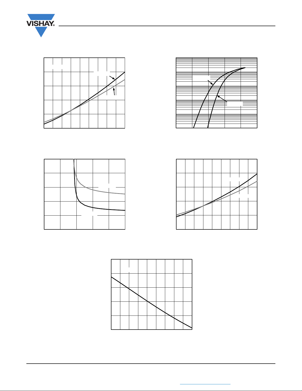
0.5
0.9
1.3
1.7
2.1
2.5
- 50 - 25 0 25 50 75 100 125 150 175
R
DS(on)
-On-Resistance (Normalized)
TJ- Junction Temperature (°C)
ID= 1.25 A
VGS= 4.5 V
VGS= 10 V
0.0
0.2
0.4
0.6
0.8
1.0
0246810
R
DS(on)
-On-Resistance (Ω)
VGS- Gate-to-Source Voltage (V)
TJ= 150 °C
TJ= 25 °C
www.vishay.com
TYPICAL CHARACTERISTICS (TA = 25 °C, unless otherwise noted)
100
10
1
SQ2309ES
Vishay Siliconix
TJ= 150 °C
On-Resistance vs. Junction Temperature
On-Resistance vs. Gate-to-Source Voltage
0.1
- Source Current (A)
S
I
0.01
0.001
0.0 0.3 0.6 0.9 1.2 1.5
VSD- Source-to-Drain Voltage (V)
TJ= 25 °C
Source Drain Diode Forward Voltage
1.0
0.7
I
= 250 μA
0.4
I
Variance (V)
0.1
GS(th)
V
-0.2
-0.5
- 50 - 25 0 25 50 75 100 125 150 175
TJ-Temperature (°C)
= 5 mA
Threshold Voltage
S11-2111-Rev. B, 07-Nov-11
THIS DOCUMENT IS SUBJECT TO CHANGE WITHOUT NOTICE. THE PRODUCTS DESCRIBED HEREIN AND THIS DOCUMENT
ARE SUBJECT TO SPECIFIC DISCLAIMERS, SET FORTH AT www.vishay.com/doc?91000
-60
-64
-68
-72
-Drain-to-Source Voltage (V)
-76
DS
V
-80
- 50 - 25 0 25 50 75 100 125 150 175
ID= 1 mA
TJ- Junction Temperature (°C)
Drain Source Breakdown vs. Junction Temperature
4
Document Number: 67024
 Loading...