

Page 1

SMF5V0A to SMF51A
Surface Mount ESD Protection Diodes
Features
• For surface mounted applications
• Low-profile package
• Optimized for LAN protection applications
• Ideal for ESD protection of data lines in
accordance with IEC 61000-4-2 (IEC801-2)
• Ideal for EFT protection of data lines in
accordance with IEC 61000-4-4 (IEC801-4)
• IEC 61000-4-2 (ESD) 15 kV (air) 8 kV (contact)
• Low incremental surge resistance, excellent
clamping capability
• 200 W peak pulse power capability with a
10/1000 µs waveform, repetition rate
(duty cycle): 0.01 %
• Very fast response time
• High temperature soldering guaranteed:
260 °C/ 10 seconds at terminals
• Lead (Pb)-free component
• Component in accordance to RoHS 2002/95/EC
and WEEE 2002/96/EC
e3
Mechanical Data
Case: JEDEC DO-219AB (SMF®) Plastic case
Terminals: Solder plated, solderable per
MIL-STD-750, Method 2026
Polarity:The band denotes the cathode, which is
positive with respect to the anode under normal
TVS operation
Mounting Position: Any
Weight: approx. 15 mg
Packaging Codes/Options:
GS18 / 10 k per 13 " reel (8 mm tape), 50 k/box
GS08 / 3 k per 7 " reel (8 mm tape), 30 k/box
Vishay Semiconductors
17249
Absolute Maximum Ratings
Ratings at 25 °C, ambient temperature unless otherwise specified
Parameter Test condition Symbol Val ue Unit
Peak pulse power dissipation
Peak pulse current
Peak forward surge current 8.3 ms single half sine-wave I
1)
Non-repetitive current pulse and derated above TA = 25 °C
10/1000 µs waveform
8/20 µs waveform
10/1000 µs waveform
1)
1)
1)
Thermal Characteristics
Ratings at 25 °C, ambient temperature unless otherwise specified
Parameter Test condition Symbol Val ue Unit
Thermal resistance
Operation junction and storage
temperature range
2) Mounted on epoxy glass PCB with 3 x 3 mm, Cu pads ( ≥ 40 µm thick)
Document Number 85811
Rev. 2.0, 29-Apr-05
2)
P
PPM
P
PPM
I
PPM
FSM
R
thJA
T
, T
stg
J
200 W
1000 W
next
Ta bl e
20 A
180 K/W
- 55 to + 150 °C
www.vishay.com
A
1
Page 2

SMF5V0A to SMF51A
Vishay Semiconductors
Electrical Characteristics
Ratings at 25 °C ambient temperature unless otherwise specified. VF = 3.5 V at IF = 12 A (uni-directional only)
Partnumber Marking
Code
UNI
SMF5V0A AE 6.40 10 5.0 400 21.7 9.2 1030
SMF6V0A AG 6.67 10 6.0 400 19.4 10.3 1010
SMF6V5A AK 7.22 10 6.5 250 17.9 11.2 850
SMF7V0A AM 7.78 10 7.0 100 16.7 12.0 750
SMF7V5A AP 8.33 1.0 7.5 50 15.5 12.9 730
SMF8V0A AR 8.89 1.0 8.0 25 14.7 13.6 670
SMF8V5A AT 9.44 1.0 8.5 10 13.9 14.4 660
SMF9V0A AV 10.0 1.0 9.0 5.0 13.5 15.4 620
SMF10A AX 11.1 1.0 10 2.5 11.8 17.0 570
SMF11A AZ 12.2 1.0 11 2.5 11.0 18.2 460
SMF12A BE 13.3 1.0 12 2.5 10.1 19.9 440
SMF13A BG 14.4 1.0 13 1.0 9.3 21.5 420
SMF14A BK 15.6 1.0 14 1.0 8.6 23.2 370
SMF15A BM 16.7 1.0 15 1.0 8.2 24.4 350
SMF16A BP 17.8 1.0 16 1.0 7.7 26.0 340
SMF17A BR 18.9 1.0 17 1.0 7.2 27.6 310
SMF18A BT 20.0 1.0 18 1.0 5.8 29.2 305
SMF20A BV 22.2 1.0 20 1.0 6.2 32.4 207
SMF22A BX 24.4 1.0 22 1.0 5.6 35.5 265
SMF24A BZ 26.7 1.0 24 1.0 5.1 38.9 240
SMF26A CE 28.9 1.0 26 1.0 4.8 42.1 225
SMF28A CG 31.1 1.0 28 1.0 4.4 45.4 210
SMF30A CK 33.3 1.0 30 1.0 4.1 48.4 205
SMF33A CM 36.7 1.0 33 1.0 3.8 53.3 190
SMF36A CP 40.0 1.0 36 1.0 3.4 58.1 180
SMF40A CR 44.4 1.0 40 1.0 3.1 64.5 165
SMF43A CT 47.8 1.0 43 1.0 2.9 69.4 160
SMF45A CV 50.0 1.0 45 1.0 2.8 72.7 155
SMF48A CX 53.3 1.0 48 1.0 2.6 77.4 150
SMF51A CZ 56.7 1.0 51 1.0 2.4 82.4 145
1)
Pulse test tp ≤ 5.0 ms
2)
Surge current waveform 10/1000 µs
3)
All terms and symbols are consistent with ANSI/IEEE C62.35
Breakdown
Voltage
V
(BR)
Test Current Stand-off
1)
@ I
T
Voltage
V
WM
Maximum
Reverse
Leakage
@ V
WM
I
D
Maximum
Peak Pulse
Surge
2,3)
Current
I
PPM
Maximum
Clamping
Voltage
@ I
PPM
V
C
V mA V µA A V pF
min typ
Capacitance
f = 1 MHz
Junction
Cj @
= 0 V,
V
R
www.vishay.com
2
Document Number 85811
Rev. 2.0, 29-Apr-05
Page 3
SMF5V0A to SMF51A
Vishay Semiconductors
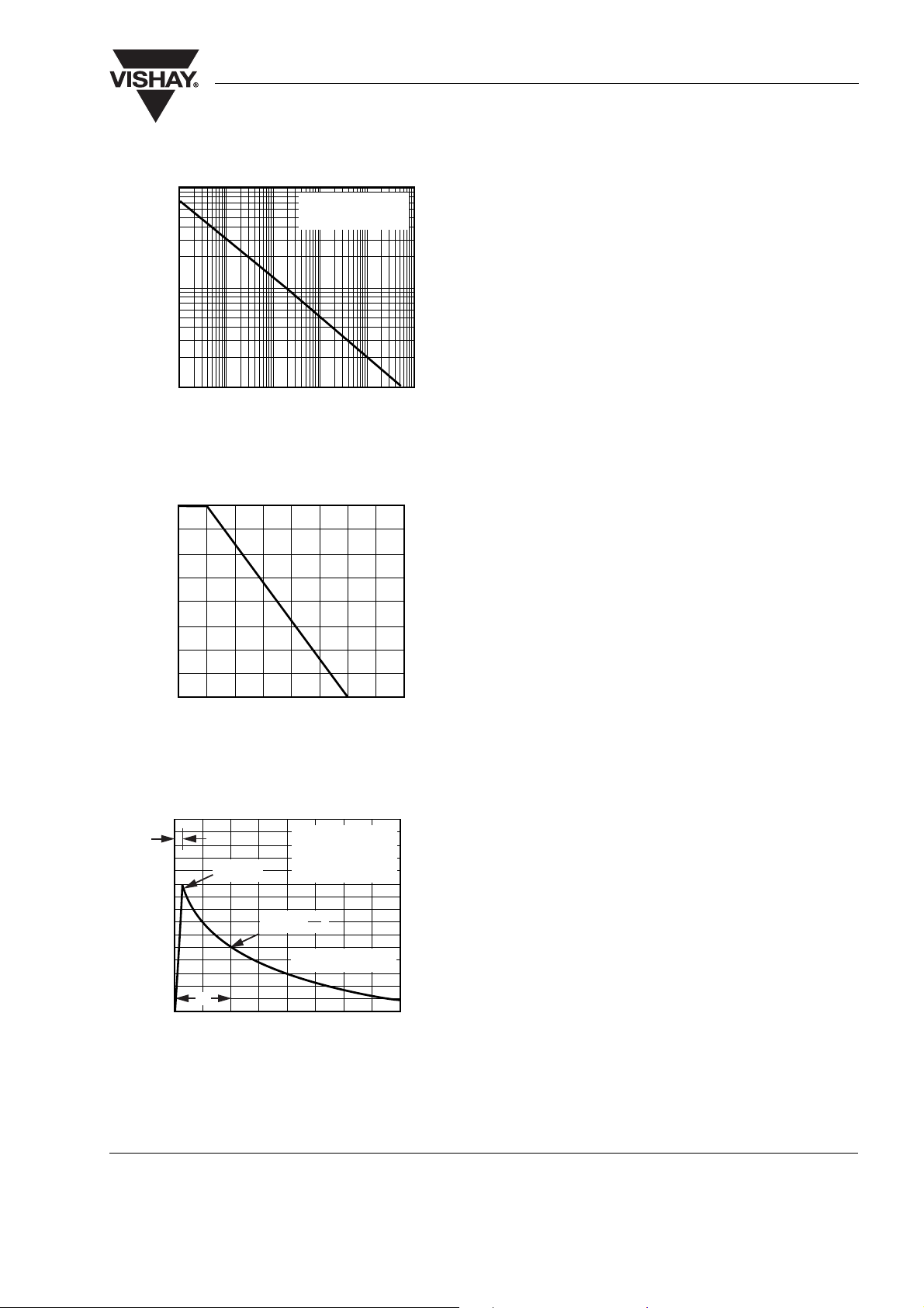
Typical Characteristics (Tamb = 25 °C unless otherwise specified)
10
1
- Peak Pulse Power (kW)
PPM
P
0.1
0.1µs 1.0µs10µs
17250
100
75
50
Non-repetitive Pulse
Waveform shown in Fig. 3
T
=25 °C
A
100µs 1.0ms 10ms
td- Pulse Width (sec.)
Figure 1. Peak Pulse Power Rating
17251
17252
Peak Pulse Power (PPP) or Current (IPPM)
RSM
- Peak Pulse Current, % I
PPM
I
Derating in Percentage, %
150
100
25
0
0
7525 50
TA- Ambient Temperature (°C)
Figure 2. Pulse Derating Curve
tr = 10 µs
Peak Value
I
PPM
Half Value - IPP
I
PPM
50
td
0
0
1.0
t - Time (ms)
Figure 3. Pulse Waveform
100 125
2.0
150 175 200
TJ=25 °C
Pulse Width (td)
is defined as the point
where the peak current
decays to 50% of I
2
10/1000sec. Waveform
as defined by R.E.A.
3.0 4.0
PPM
Document Number 85811
Rev. 2.0, 29-Apr-05
www.vishay.com
3
Page 4

SMF5V0A to SMF51A
Vishay Semiconductors
Package Dimensions in mm (Inches)
5
0.85 (0.033)
0.35 (0.014)
3.9 (0.152)
3.5 (0.137)
Detail
Z
enlarged
ISO Method E
0.10 max
5
0.99 (0.039)
0.97 (0.038)
1.9 (0.074)
1.7 (0.066)
0.16 (0.006)
Z
Cathode Band
Top View
1.2 (0.047)
0.8 (0.031)
2.9 (0.113)
2.7 (0.105)
Mounting Pad Layout
1.6 (0.062) 1.3 (0.051)
www.vishay.com
4
1.4 (0.055)
17247
Document Number 85811
Rev. 2.0, 29-Apr-05
Page 5

Blistertape for SMF
SMF5V0A to SMF51A
Vishay Semiconductors
PS
18513
Document Number 85811
Rev. 2.0, 29-Apr-05
www.vishay.com
5
Page 6

SMF5V0A to SMF51A
Vishay Semiconductors
Ozone Depleting Substances Policy Statement
It is the policy of Vishay Semiconductor GmbH to
1. Meet all present and future national and international statutory requirements.
2. Regularly and continuously improve the performance of our products, processes, distribution and operating
systems with respect to their impact on the health and safety of our employees and the public, as well as
their impact on the environment.
It is particular concern to control or eliminate releases of those substances into the atmosphere which are
known as ozone depleting substances (ODSs).
The Montreal Protocol (1987) and its London Amendments (1990) intend to severely restrict the use of ODSs
and forbid their use within the next ten years. Various national and international initiatives are pressing for an
earlier ban on these substances.
Vishay Semiconductor GmbH has been able to use its policy of continuous improvements to eliminate the use
of ODSs listed in the following documents.
1. Annex A, B and list of transitional substances of the Montreal Protocol and the London Amendments
respectively
2. Class I and II ozone depleting substances in the Clean Air Act Amendments of 1990 by the Environmental
Protection Agency (EPA) in the USA
3. Council Decision 88/540/EEC and 91/690/EEC Annex A, B and C (transitional substances) respectively.
Vishay Semiconductor GmbH can certify that our semiconductors are not manufactured with ozone depleting
substances and do not contain such substances.
We reserve the right to make changes to improve technical design
and may do so without further notice.
Parameters can vary in different applications. All operating parameters must be validated for each
customer application by the customer. Should the buyer use Vishay Semiconductors products for any
unintended or unauthorized application, the buyer shall indemnify Vishay Semiconductors against all
claims, costs, damages, and expenses, arising out of, directly or indirectly, any claim of personal
damage, injury or death associated with such unintended or unauthorized use.
Vishay Semiconductor GmbH, P.O.B. 3535, D-74025 Heilbronn, Germany
www.vishay.com
6
Document Number 85811
Rev. 2.0, 29-Apr-05
Page 7

WWW.ALLDATASHEET.COM
Copyright © Each Manufacturing Company.
All Datasheets cannot be modified without permission.
This datasheet has been download from :
www.AllDataSheet.com
100% Free DataSheet Search Site.
Free Download.
No Register.
Fast Search System.
www.AllDataSheet.com
 Loading...