

www.vishay.com
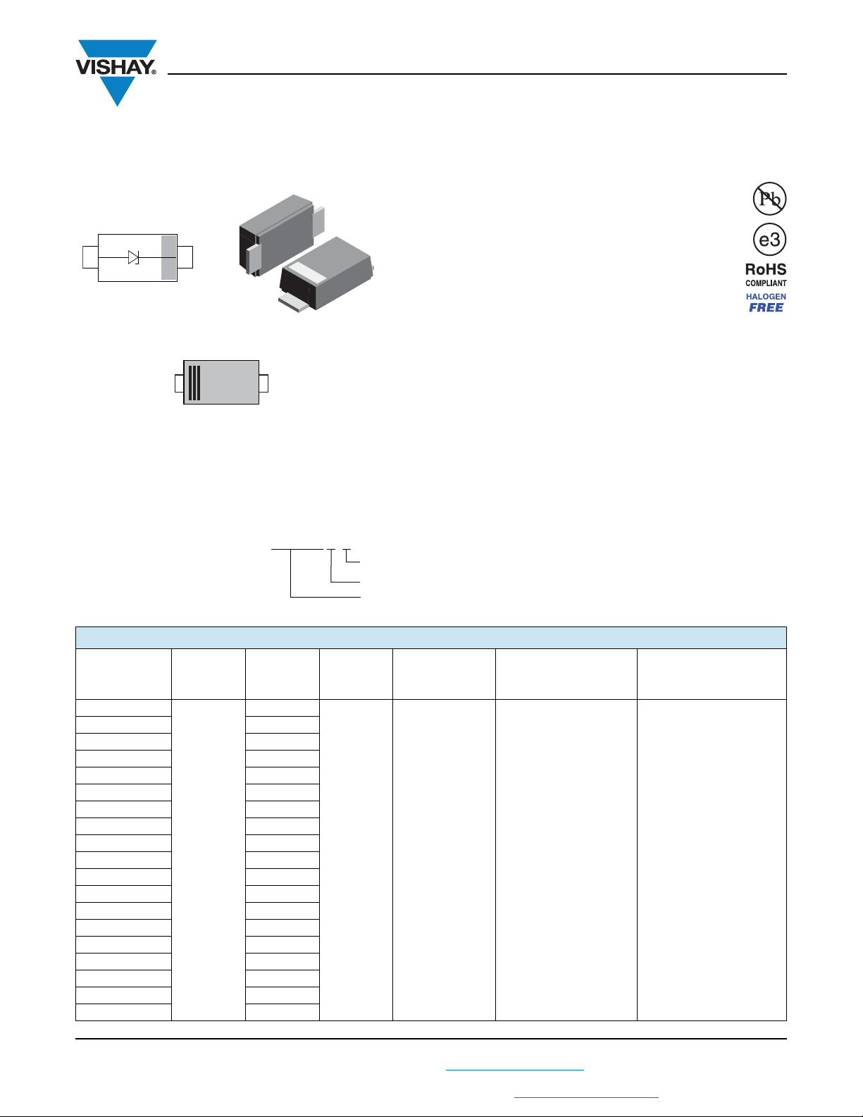
Surface Mount ESD Protection Diodes
20278
2
17249
XX
YY
1
MARKING (example only)
Bar = cathode marking
YY = type code (see table below)
XX = date code
ORDERING INFORMATION
22623
SMF5V0A-M-xx
SMF5V0A-M to SMF51A-M
Vishay Semiconductors
FEATURES
• For surface mounted applications
• Low-profile package
• Optimized for LAN protection applications
• Ideal for ESD protection of data lines in
accordance with IEC 61000-4-2 (IEC 801-2)
• Ideal for EFT protection of data lines in
accordance with IEC 61000-4-4 (IEC 801-4)
• ESD-protection acc. IEC 61000-4-2
± 30 kV contact discharge
± 30 kV air discharge
• Low incremental surge resistance, excellent clamping
capability
• 200 W peak pulse power capability with a 10/1000 μs
waveform, repetition rate (duty cycle): 0.01 %
• Very fast response time
• High temperature soldering guaranteed: 260 °C/10 s at
terminals
•e3 - Sn
• AEC-Q101 qualified
• Compliant to RoHS Directive 2002/95/EC and in
accordance to WEEE 2002/96/EC
• Halogen-free according to IEC 61249-2-21 definiton
08 = 3K per 7" reel (8 mm tape), 30K/box
18 = 10K per 13" reel (8 mm tape), 50K/box
Environmental suffix -M- defines halogen-free
Part number
PACKAGE DATA
MOLDING
DEVICE NAME
SMF5V0A-M
SMF6V5A-M NK
SMF7V0A-M NM
SMF7V5A-M NP
SMF8V0A-M NR
SMF8V5A-M NT
SMF9V0A-M NV
SMF10A-M NX
SMF11A-M NZ
SMF12A-M OE
SMF13A-M OG
SMF14A-M OK
SMF15A-M OM
SMF16A-M OP
SMF17A-M OR
SMF18A-M OT
SMF20A-M OV
SMF22A-M OX
SMF24A-M OZ
Rev. 1.1, 30-Nov-11
THIS DOCUMENT IS SUBJECT TO CHANGE WITHOUT NOTICE. THE PRODUCTS DESCRIBED HEREIN AND THIS DOCUMENT
PACKAGE
NAME
SMF
ARE SUBJECT TO SPECIFIC DISCLAIMERS, SET FORTH AT www.vishay.com/doc?91000
TYPE CODE WEIGHT
NE
15 mg UL 94 V-0
For technical questions, contact: ESDprotection@vishay.com
COMPOUND
FLAMMABILITY
RATING
1
MOISTURE SENSITIVITY
LEVEL
MSL level 1
(according J-STD-020)
SOLDERING CONDITIONS
260 °C/10 s at terminals
Document Number: 83355
www.vishay.com
PACKAGE DATA
DEVICE NAME
PACKAGE
NAME
SMF26A-M
SMF28A-M PG
SMF30A-M PK
SMF33A-M PM
SMF36A-M PP
SMF40A-M PR
SMF
SMF43A-M PT
SMF45A-M PV
SMF48A-M PX
SMF51A-M PZ
TYPE CODE WEIGHT
PE
MOLDING
COMPOUND
FLAMMABILITY
RATING
15 mg UL 94 V-0
SMF5V0A-M to SMF51A-M
Vishay Semiconductors
MOISTURE SENSITIVITY
LEVEL
MSL level 1
(according J-STD-020)
SOLDERING CONDITIONS
260 °C/10 s at terminals
ABSOLUTE MAXIMUM RATINGS (T
= 25 °C, unless otherwise specified)
amb
PARAMETER TEST CONDITIONS SYMBOL VALUE UNIT
Peak pulse current t
Peak pulse power
= 10/1000 μs waveform acc. IEC 61000-4-5 I
p
t
= 8/20 μs waveform acc. IEC 61000-4-5
p
= 10/1000 μs waveform acc. IEC 61000-4-5 200 W
t
p
Peak forward surge current 8.3 ms single half sine-wave I
ESD immunity
Thermal resistance
Forward clamping voltage I
Contact discharge acc. IEC 61000-4-2; 10 pulses
Air discharge acc. IEC 61000-4-2; 10 pulses ± 30 kV
Mounted on epoxy glass PCB with 3 mm x 3 mm,
Cu pads ( 40 μm thick)
= 12 A V
F
Operating temperature Junction temperature T
Storage temperature T
ELECTRICAL CHARACTERISTICS (T
PART
NUMBER
REVERSE
BREAKDOWN
VOLTAGE
, tp 5 ms
at I
T
MIN.
V
BR
(V)
TEST
CURRENT
IT
(mA)
= 25 °C, unless otherwise specified)
amb
REVERSE
WORKING
VOLTAGE
V
RWM
(V)
REVERSE
CURRENT
at V
RWM
IR
(μA)
MAXIMUM
PEAK PULSE
CURRENT
t
= 10/1000 μs
p
I
PPM
(A)
PPM
P
PP
FSM
V
ESD
R
thJA
F
J
STG
REVERSE
CLAMPING
VOLTAGE
at I
PPM
VC
(V)
see “Electrical
Characteristics”
1000 W
20 A
± 30 kV
180 K/W
3.5 V
- 55 to + 150 °C
- 55 to + 150 °C
CAPACITANCE
at VR = 0 V,
f = 1 MHz
CD TYP.
(pF)
A
PROTECTION
PATHS
N
channel
SMF5V0A-M 6.40 10 5 400 21.7 9.2 1030 1
SMF6V0A-M 6.67 10 6 400 19.4 10.3 1010 1
SMF6V5A-M 7.22 10 6.5 250 17.9 11.2 850 1
SMF7V0A-M 7.78 10 7 100 16.7 12 750 1
SMF7V5A-M 8.33 1 7.5 50 15.5 12.9 730 1
SMF8V0A-M 8.89 1 8 25 14.7 13.6 670 1
SMF8V5A-M 9.44 1 8.5 10 13.9 14.4 660 1
SMF9V0A-M 10 1 9 5 13.5 15.4 620 1
SMF10A-M 11.1 1 10 2.5 11.8 17 570 1
SMF11A-M 12.2 1 11 2.5 11 18.2 460 1
SMF12A-M 13.3 1 12 2.5 10.1 19.9 440 1
SMF13A-M 14.4 1 13 1 9.3 21.5 420 1
SMF14A-M 15.6 1 14 1 8.6 23.2 370 1
SMF15A-M 16.7 1 15 1 8.2 24.4 350 1
SMF16A-M 17.8 1 16 1 7.7 26 340 1
SMF17A-M 18.9 1 17 1 7.2 27.6 310 1
SMF18A-M 20 1 18 1 5.8 29.2 305 1
Rev. 1.1, 30-Nov-11
2
Document Number: 83355
For technical questions, contact: ESDprotection@vishay.com
THIS DOCUMENT IS SUBJECT TO CHANGE WITHOUT NOTICE. THE PRODUCTS DESCRIBED HEREIN AND THIS DOCUMENT
ARE SUBJECT TO SPECIFIC DISCLAIMERS, SET FORTH AT www.vishay.com/doc?91000
www.vishay.com
SMF5V0A-M to SMF51A-M
Vishay Semiconductors
ELECTRICAL CHARACTERISTICS (T
PART
NUMBER
REVERSE
BREAKDOWN
VOLTAGE
, tp 5 ms
at I
T
MIN.
V
BR
(V)
TEST
CURRENT
IT
(mA)
= 25 °C, unless otherwise specified)
amb
REVERSE
WORKING
VOLTAGE
V
RWM
(V)
REVERSE
CURRENT
at V
RWM
IR
(μA)
MAXIMUM
PEAK PULSE
CURRENT
t
= 10/1000 μs
p
I
PPM
(A)
REVERSE
CLAMPING
VOLTAGE
at I
PPM
VC
(V)
CAPACITANCE
at VR = 0 V,
f = 1 MHz
CD TYP.
(pF)
PROTECTION
SMF20A-M 22.2 1 20 1 6.2 32.4 207 1
SMF22A-M 24.4 1 22 1 5.6 35.5 265 1
SMF24A-M 26.7 1 24 1 5.1 38.9 240 1
SMF26A-M 28.9 1 26 1 4.8 42.1 225 1
SMF28A-M 31.1 1 28 1 4.4 45.4 210 1
SMF30A-M 33.3 1 30 1 4.1 48.4 205 1
SMF33A-M 36.7 1 33 1 3.8 53.3 190 1
SMF36A-M 40 1 36 1 3.4 58.1 180 1
SMF40A-M 44.4 1 40 1 3.1 64.5 165 1
SMF43A-M 47.8 1 43 1 2.9 69.4 160 1
SMF45A-M 50 1 45 1 2.8 72.7 155 1
SMF48A-M 53.3 1 48 1 2.6 77.4 150 1
SMF51A-M 56.7 1 51 1 2.4 82.4 145 1
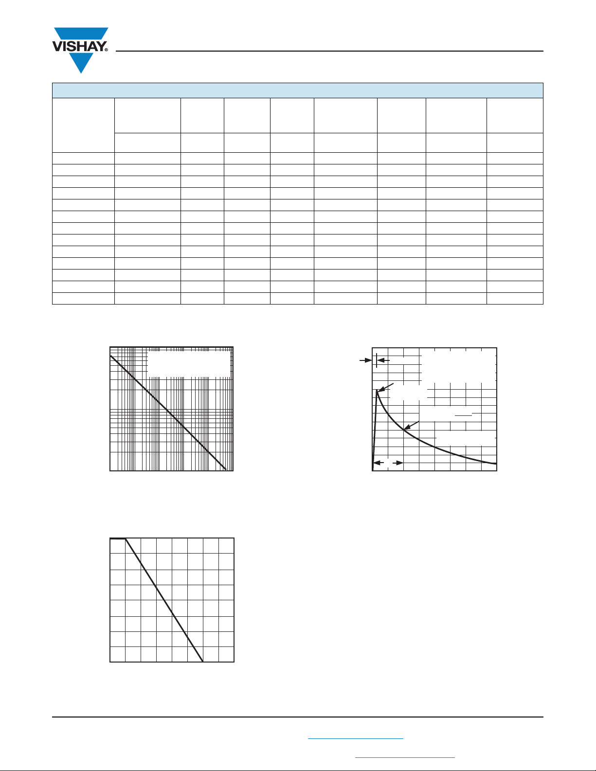
TYPICAL CHARACTERISTICS (T
10
1
- Peak Pulse Power (kW)
PP
P
0.1
0.1 µs 1.0 µs 10 µs
17250
Fig. 1 - Peak Pulse Power Rating
Non-repetitive pulse
waveform shown in fig. 3
= 25 °C
T
A
100 µs 1.0 ms 10 ms
t
- Pulse Width (s)
d
= 25 °C, unless otherwise specified)
amb
150
RSM
100
- Peak Pulse Current, % I
PPM
I
17252
tr=10 µs
Peak value
I
50
t
d
0
0 1 2 3 4
TJ = 25 °C
pulse width (t
defined as the point
where the peak current
decays to 50 % of I
PPM
Half value
I
PPM
t - Time (ms)
10/100 s waveform
as defined by R.E.A.
Fig. 3 - Pulse Waveform
I
PPM
) is
d
PPM
2
PATHS
N
channel
)
100
PPM
75
) or Current (I
PP
50
25
Derating in Percentage (%)
0
Peak Pulse Power (P
0
17251
7525 50
100 125 150 175 200
TA - Ambient Temperature
Fig. 2 - Pulse Derating Curve
Rev. 1.1, 30-Nov-11
3
Document Number: 83355
For technical questions, contact: ESDprotection@vishay.com
THIS DOCUMENT IS SUBJECT TO CHANGE WITHOUT NOTICE. THE PRODUCTS DESCRIBED HEREIN AND THIS DOCUMENT
ARE SUBJECT TO SPECIFIC DISCLAIMERS, SET FORTH AT www.vishay.com/doc?91000

www.vishay.com
PACKAGE DIMENSIONS in millimeters (inches): SMF
0.85 (0.033)
0.35 (0.014)
0.05 (0.002)
0.25 (0.010)
1.9 (0.075)
1.7 (0.067)
SMF5V0A-M to SMF51A-M
Vishay Semiconductors
Detail Z
enlarged
0 (0.000)
0.1 (0.004)
5
0.8 (0.031)
1.2 (0.047)
5
Created - Date: 15. February 2005
Rev. 3 - Date: 13. March 2007
Document no.:S8-V-3915.01-001 (4)
17247
2.9 (0.114)
2.7 (0.106)
3.9 (0.154)
3.5 (0.138)
1.08 (0.043)
0.88 (0.035)
Foot print recommendation:
1.3 (0.051) 1.3 (0.051)
1.4 (0.055)
2.9 (0.114)
Rev. 1.1, 30-Nov-11
4
Document Number: 83355
For technical questions, contact: ESDprotection@vishay.com
THIS DOCUMENT IS SUBJECT TO CHANGE WITHOUT NOTICE. THE PRODUCTS DESCRIBED HEREIN AND THIS DOCUMENT
ARE SUBJECT TO SPECIFIC DISCLAIMERS, SET FORTH AT www.vishay.com/doc?91000

www.vishay.com
18513
PS
Document-No.: S8-V-3717.02-001 (3)
BLISTERTAPE DIMENSIONS in millimeters (inches)
SMF5V0A-M to SMF51A-M
Vishay Semiconductors
Rev. 1.1, 30-Nov-11
THIS DOCUMENT IS SUBJECT TO CHANGE WITHOUT NOTICE. THE PRODUCTS DESCRIBED HEREIN AND THIS DOCUMENT
5
For technical questions, contact: ESDprotection@vishay.com
ARE SUBJECT TO SPECIFIC DISCLAIMERS, SET FORTH AT www.vishay.com/doc?91000
Document Number: 83355

www.vishay.com
Pin 1 - Location
Top view Pad layout - view from top
seen at bottom side
LLP1713
LLP2513
LLP3313
Pin 1 - Location
Pin 1 - Location
Top view
Top view
Pad layout - view from top
seen at bottom side
Pad layout - view from top
seen at bottom side
SMF5V0A-M to SMF51A-M
Vishay Semiconductors
Rev. 1.1, 30-Nov-11
6
Document Number: 83355
For technical questions, contact: ESDprotection@vishay.com
THIS DOCUMENT IS SUBJECT TO CHANGE WITHOUT NOTICE. THE PRODUCTS DESCRIBED HEREIN AND THIS DOCUMENT
ARE SUBJECT TO SPECIFIC DISCLAIMERS, SET FORTH AT www.vishay.com/doc?91000

Legal Disclaimer Notice
www.vishay.com
Vishay
Disclaimer
ALL PRODUCT, PRODUCT SPECIFICATIONS AND DATA ARE SUBJECT TO CHANGE WITHOUT NOTICE TO IMPROVE
RELIABILITY, FUNCTION OR DESIGN OR OTHERWISE.
Vishay Intertechnology, Inc., its affiliates, agents, and employees, and all persons acting on its or their behalf (collectively,
“Vishay”), disclaim any and all liability for any errors, inaccuracies or incompleteness contained in any datasheet or in any other
disclosure relating to any product.
Vishay makes no warranty, representation or guarantee regarding the suitability of the products for any particular purpose or
the continuing production of any product. To the maximum extent permitted by applicable law, Vishay disclaims (i) any and all
liability arising out of the application or use of any product, (ii) any and all liability, including without limitation special,
consequential or incidental damages, and (iii) any and all implied warranties, including warranties of fitness for particular
purpose, non-infringement and merchantability.
Statements regarding the suitability of products for certain types of applications are based on Vishay’s knowledge of typical
requirements that are often placed on Vishay products in generic applications. Such statements are not binding statements
about the suitability of products for a particular application. It is the customer’s responsibility to validate that a particular
product with the properties described in the product specification is suitable for use in a particular application. Parameters
provided in datasheets and/or specifications may vary in different applications and performance may vary over time. All
operating parameters, including typical parameters, must be validated for each customer application by the customer’s
technical experts. Product specifications do not expand or otherwise modify Vishay’s terms and conditions of purchase,
including but not limited to the warranty expressed therein.
Except as expressly indicated in writing, Vishay products are not designed for use in medical, life-saving, or life-sustaining
applications or for any other application in which the failure of the Vishay product could result in personal injury or death.
Customers using or selling Vishay products not expressly indicated for use in such applications do so at their own risk. Please
contact authorized Vishay personnel to obtain written terms and conditions regarding products designed for such applications.
No license, express or implied, by estoppel or otherwise, to any intellectual property rights is granted by this document or by
any conduct of Vishay. Product names and markings noted herein may be trademarks of their respective owners.
Material Category Policy
Vishay Intertechnology, Inc. hereby certifies that all its products that are identified as RoHS-Compliant fulfill the
definitions and restrictions defined under Directive 2011/65/EU of The European Parliament and of the Council
of June 8, 2011 on the restriction of the use of certain hazardous substances in electrical and electronic equipment
(EEE) - recast, unless otherwise specified as non-compliant.
Please note that some Vishay documentation may still make reference to RoHS Directive 2002/95/EC. We confirm that
all the products identified as being compliant to Directive 2002/95/EC conform to Directive 2011/65/EU.
Vishay Intertechnology, Inc. hereby certifies that all its products that are identified as Halogen-Free follow Halogen-Free
requirements as per JEDEC JS709A standards. Please note that some Vishay documentation may still make reference
to the IEC 61249-2-21 definition. We confirm that all the products identified as being compliant to IEC 61249-2-21
conform to JEDEC JS709A standards.
Revision: 02-Oct-12
1
Document Number: 91000

 Loading...