

SiP32431
SiP32431
IN
V
OUT
OUT
V
IN
GND
GND
GND
ON/OFF
ON/OFF
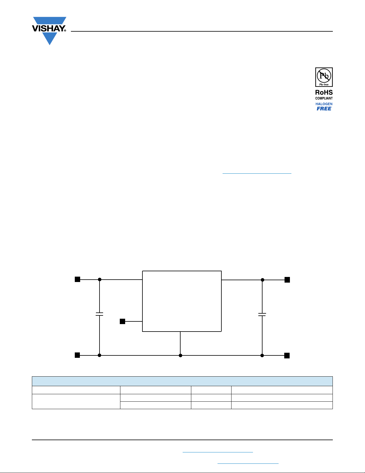
C
1 µF
IN
C
0.1 µF
OUT
www.vishay.com
Vishay Siliconix
1 A Slew Rate Controlled Load Switch with Reverse Blocking
DESCRIPTION
The SiP32431 is a slew rate controlled high side switch with
reverse blocking capability. The switch is of a low ON
resistance p-channel MOSFET that supports continuous
current up to 1 A.
The SiP32431 operates with an input voltage from 1.5 V to
5.5 V.
The SiP32431 features low input logic level to interface with
low control voltage from microprocessors. This device has a
very low operating current, typically 50 pA.
The SiP32431 is available in lead (Pb)-free package options
including 6 pin SC70-6, and 4 pin TDFN4 1.2 mm x 1.6 mm
DFN4 packages. The operation temperature range is
specified from -40 °C to +85 °C.
The SiP32431 compact package options, operation voltage
range, and low operating current make it a good fit for
battery power applications.
FEATURES
• 1.5 V to 5.5 V input voltage range
• Very low R
, typically 105 mΩ at 5 V and
DS(on)
135 mΩ at 3 V for TDFN4 1.2 mm x 1.6 mm
package
• Typical 147 mΩ at 5 V and 178 mΩ at 3 V for
SC70-6 package
Available
• Slew rate controlled turn-on time: 100 μs
• Low quiescent current < 1 μA
• Low shutdown current < 1 μA
• Reverse blocking capability
• SC70-6 and TDFN4 1.2 mm x 1.6 mm packages
• Material categorization: for definitions of compliance
please see www.vishay.com/doc?99912
APPLICATIONS
• Cellular telephones
• Digital still cameras
• Personal digital assistants (PDA)
• Hot swap supplies
• Notebook computers
• Personal communication devices
• Portable Instruments
TYPICAL APPLICATION CIRCUIT
Fig. 1 - SiP32431 Typical Application Circuit
ORDERING INFORMATION
TEMPERATURE RANGE PACKAGE MARKING PART NUMBER
-40 °C to 85 °C
Notes
•x = lot code
• -GE3 denotes halogen-free and RoHS-compliant
• Please use the SiP32431DR3-T1GE3 to replace SiP32431DR3-T1-E3
S15-1821-Rev. C, 10-Aug-15
THIS DOCUMENT IS SUBJECT TO CHANGE WITHOUT NOTICE. THE PRODUCTS DESCRIBED HEREIN AND THIS DOCUMENT
TDFN4 1.2 mm x 1.6 mm Dx SiP32431DNP3-T1GE4
For technical questions, contact: powerictechsupport@vishay.com
ARE SUBJECT TO SPECIFIC DISCLAIMERS, SET FORTH AT www.vishay.com/doc?91000
SC70-6 MAxx SiP32431DR3-T1GE3
1
Document Number: 66597
SiP32431
www.vishay.com
ABSOLUTE MAXIMUM RATINGS
PARAMETER LIMIT UNIT
Supply Input Voltage (V
Output Voltage (V
Maximum Continuous Switch Current (I
Maximum Pulsed Current (I
(pulsed at 1 ms, 10 % duty cycle)
ESD Rating (HBM) 4000 V
Junction Temperature (T
Thermal Resistance (θ
Power Dissipation (P
Notes
a. Device mounted with all leads and power pad soldered or welded to PC board.
b. Derate 4.5 mW/°C above T
c. Derate 5.9 mW/°C above T
Stresses beyond those listed under "Absolute Maximum Ratings" may cause permanent damage to the device. These are stress ratings only, and functional operation
of the device at these or any other conditions beyond those indicated in the operational sections of the specifications is not implied. Exposure to absolute maximum
rating/conditions for extended periods may affect device reliability.
) -0.3 to 6
IN
) -0.3 to 6
ON/OFF
) -0.3 to VIN +0.3
OUT
)
max.
) VIN
DM
) -40 to 125 °C
J
a
)
JA
a
)
D
= 70 °C.
A
= 70 °C, see PCB layout.
A
SC70-6 package 1.2
TDFN4 1.2 mm x 1.6 mm 1.4
V
≥ 2.5 V 3
IN
V
< 2.5 V 1.6
IN
6 pin SC70-6
4 pin TDFN4 1.2 mm x 1.6 mm
6 pin SC70- 6
4 pin TDFN4 1.2 mm x 1.6 mm
b
c
b
c
220
170
250
324
Vishay Siliconix
VEnable Input Voltage (V
A
°C/W
mW
RECOMMENDED OPERATING RANGE
PARAMETER LIMIT UNIT
Input Voltage Range (V
Operating Temperature Range -40 to 85 °C
) 1.5 to 5.5 V
IN
S15-1821-Rev. C, 10-Aug-15
2
Document Number: 66597
For technical questions, contact: powerictechsupport@vishay.com
THIS DOCUMENT IS SUBJECT TO CHANGE WITHOUT NOTICE. THE PRODUCTS DESCRIBED HEREIN AND THIS DOCUMENT
ARE SUBJECT TO SPECIFIC DISCLAIMERS, SET FORTH AT www.vishay.com/doc?91000
www.vishay.com
OUT
1
GND
2
ON/OFF
3
N/C
6
GND
5
IN
4
Top View
SPECIFICATIONS
PARAMETER SYMBOL
Operating Voltage
Quiescent Current I
Off Supply Current I
Off Switch Current I
Reverse Blocking Current I
c
V
IN
Q
Q(off)
SD(off)
RB
V
On-Resistance R
DS(on)
V
V
On-Resistance Temp.-Coefficient TD
RDS
VIN = 5, TA = -40 °C to 85 °C
(Typical values are at T
= 25 °C)
A
On/off = active - 0.00005 1
On/off = inactive, out = open - - 1
On/off = inactive, out = 0 - - 1
V
= 5.5 V, VIN = 0, V
OUT
VIN = 5 V, IL = 500 mA, TA = 25 °C
= 4.2 V, IL = 500 mA, TA = 25 °C
IN
= 3 V, IL = 500 mA, TA = 25 °C
V
IN
= 1.8 V, IL = 500 mA, TA = 25 °C
IN
= 1.5 V, IL = 500 mA, TA = 25 °C
IN
= inactive - 0.13 1
on/off
SC70-6 - 147
TDFN4 - 105
SC70-6 - 155
TDFN4 - 110
SC70-6 - 178
TDFN4 - 135
SC70-6 - 275
TDFN4 - 230
SC70-6 - 395
TDFN4 - 350
VIN ≥ 1.5 V to < 1.8 V - - 0.3
TEST CONDITIONS UNLESS SPECIFIED
On/Off Input Low Voltage
c
V
IL
V
≥ 1.8 V to < 2.7 V - - 0.4
IN
V
≥ 2.7 V to ≤ 5.5 V - - 0.6
IN
VIN ≥ 1.5 V to < 2.7 V 1.3 - -
V
On/Off Input Low Voltage c V
On/Off Input Leakage I
Output Turn-On Delay Time t
Output Turn-Off Delay Time t
SINK
d(on)
(on)
d(off)
IH
VIN = 5 V, R
≥ 2.7 V to < 4.2 V 1.5 - -
IN
V
≥ 4.2 V to ≤ 5.5 V 1.8 - -
IN
V
= 5.5 V - - 1 μA
On/Off
= 10 Ω, TA = 25 °C
load
Notes
a. The algebriac convention whereby the most negative value is a minimum and the most positive a maximum.
b. Typical values are for DESIGN AID ONLY, not guaranteed nor subject to production testing
c. For V
outside this range consult typical on/off threshold curve.
IN
-40 °C TO 85 °C
a
MIN.
TYP. bMAX.
1.5 - 5.5 V
- 2800 - ppm/°C
-2040
- 140 180
-410
SiP32431
Vishay Siliconix
LIMITS
a
230
250
290
480
520
UNIT
μA
mΩ
V
μsOutput Turn-On Rise Time t
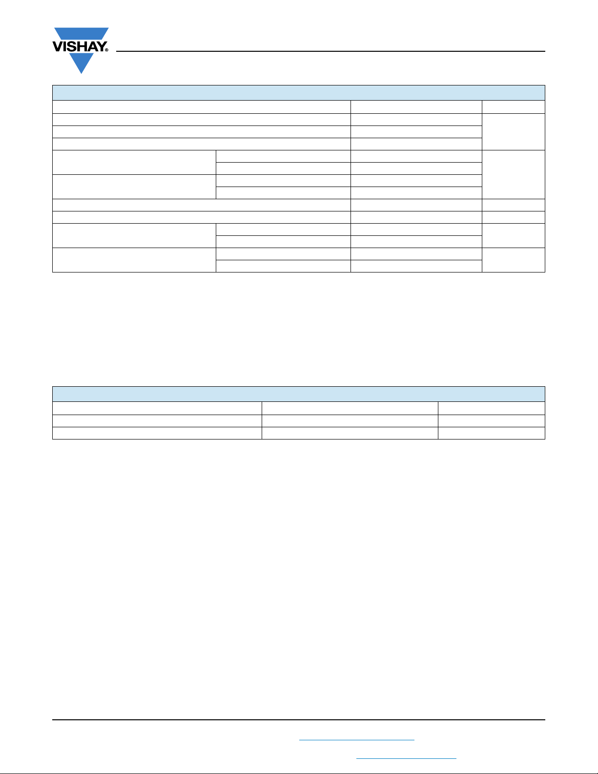
PIN CONFIGURATION
Fig. 2 - SC70-6 Package Fig. 3 - TDFN4 1.2 mm x 1.6 mm Package
PIN DESCRIPTION
PIN NUMBER
SC70-6 TDFN4
4 3 IN This pin is the p-channel MOSFET source connection. Bypass to ground through a 1 μF capacitor
2, 5 2 GND Ground connection
3 4 ON/OFF Enable input
1 1 OUT This pin is the p-channel MOSFET drain connection. Bypass to ground through a 0.1 μF capacitor
S15-1821-Rev. C, 10-Aug-15
THIS DOCUMENT IS SUBJECT TO CHANGE WITHOUT NOTICE. THE PRODUCTS DESCRIBED HEREIN AND THIS DOCUMENT
ON/OFF
4
GND
IN
3
Bottom View
NAME FUNCTION
3
For technical questions, contact: powerictechsupport@vishay.com
ARE SUBJECT TO SPECIFIC DISCLAIMERS, SET FORTH AT www.vishay.com/doc?91000
OUT
1
2
GND
Document Number: 66597
www.vishay.com
0
1.5 2.0 2.5 3.5 4.5 5.53.0 4.0 5.0
0.04
0.02
0.06
0.08
0.10
0.12
VIN (V)
I
Q
- Quiescent Current (nA)
0
1.5 2.0 2.5 3.5 5.0 6.03.0 4.0 5.54.5
150
50
250
200
100
300
350
VIN (V)
I
SD(OFF)
- Off Switch Current (nA)
0
- 40 - 20 0 40 10020 60 80
150
50
250
200
100
300
Temperature (°C)
I
SD(OFF)
- Off Switch Current (nA)
VIN = 5 V
1.0 1.5 2.0 3.0 4.0 5.52.5 3.5 4.5 5.0
V
IN
(V)
R
DS
- On-Resistance (mΩ)
50
100
150
200
250
300
350
400
450
500
550
for SC70-6 package
IL= 1.2 A
IL= 500 mA
IL= 100 mA
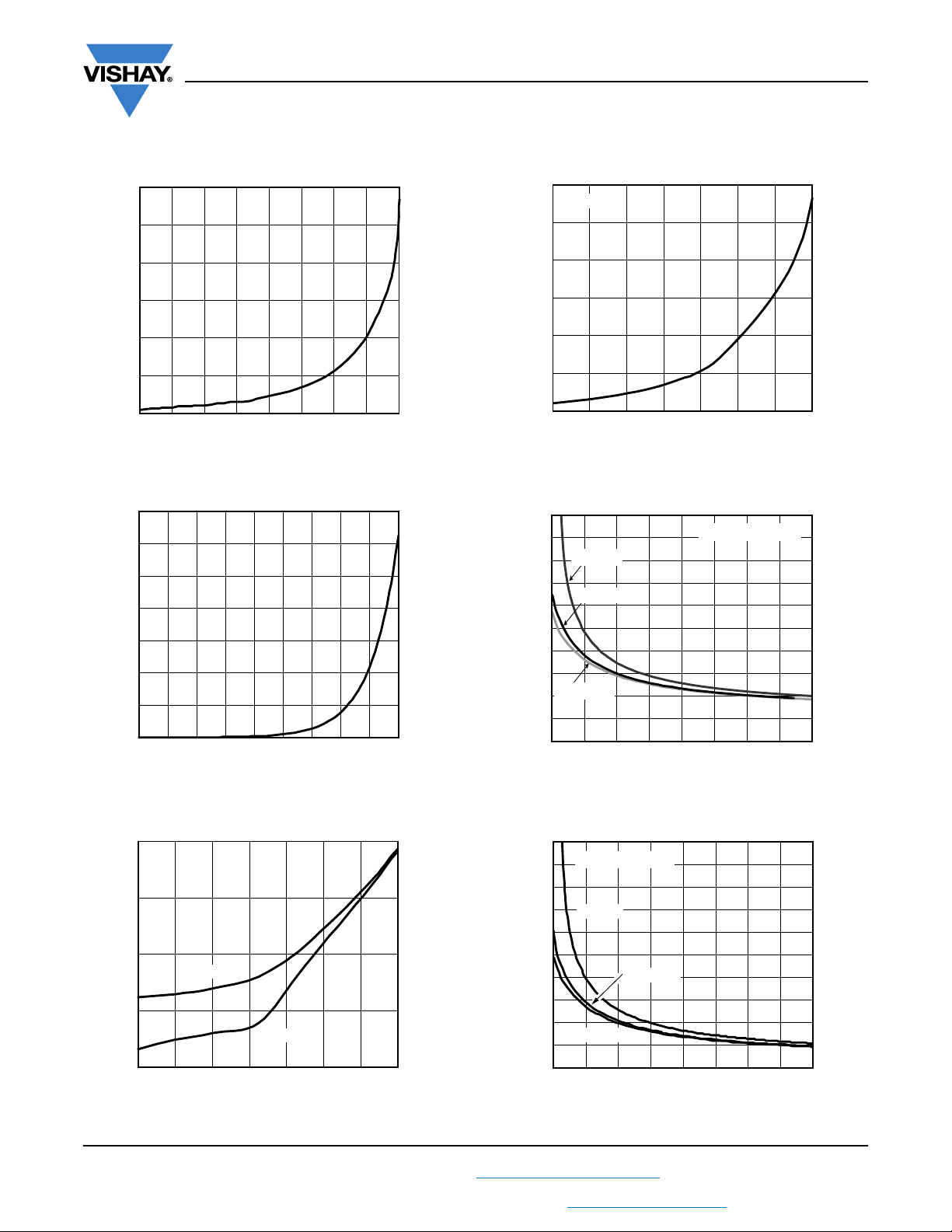
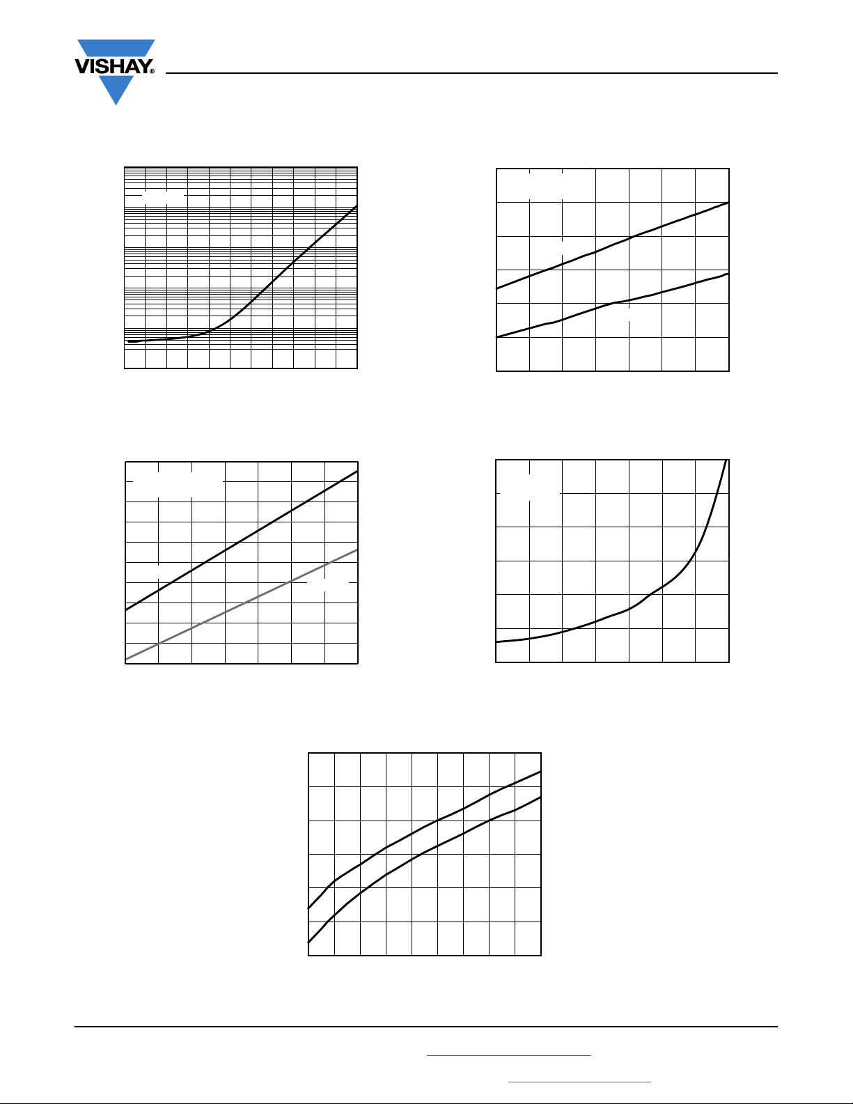
TYPICAL CHARACTERISTICS (internally regulated, 25 °C, unless otherwise noted)
SiP32431
Vishay Siliconix
Fig. 4 - Quiescent Current vs. Input Voltage
Fig. 5 - Off Switch Current vs. Input Voltage
10
1
0.1
VIN = 5 V
- Quiescent Current (nA)
Q
0.01
I
0.001
- 40 - 20 0 40 80 10020 60
Fig. 6 - Quiescent Current vs. Temperature
S15-1821-Rev. C, 10-Aug-15
THIS DOCUMENT IS SUBJECT TO CHANGE WITHOUT NOTICE. THE PRODUCTS DESCRIBED HEREIN AND THIS DOCUMENT
Fig. 7 - Off Switch Current vs. Temperature
VIN = 3 V
Temperature (°C)
Fig. 8 - R
550
500
450
400
350
300
250
- On-Resistance (mΩ)
200
DS
R
150
100
for TDFN4 package
IL = 1.2 A
IL = 100 mA
50
1.5 2.0 2.5 3.5 5.53.0 4.0 4.5 5.0
Fig. 9 - R
vs. VIN for SC70-6 Package
DS(on)
IL = 500 mA
VIN (V)
vs. Input Voltage
DS(on)
4
For technical questions, contact: powerictechsupport@vishay.com
ARE SUBJECT TO SPECIFIC DISCLAIMERS, SET FORTH AT www.vishay.com/doc?91000
Document Number: 66597
www.vishay.com
V
OUT
(V)
I
RB
- Reverse Blocking Current (nA)
0.01
0.1
1
10
100
1000
0 0.5 1 1.5 2 2.5 3 3.5 4 4.5 5 5.5
VIN = 0 V
- 40 - 20 0 40 80 10020 60
Temperature (°C)
R
DS
- On-Resistance (mΩ)
120
130
140
150
160
170
180
190
200
210
220
VIN = 5 V
VIN = 3 V
I
LOAD
= 500 mA
for SC70-6 package
60
- 40 - 20 0 40 10020 60 80
140
80
100
180
120
160
Temperature (°C)
R
DS
- On-Resistance (mΩ)
VIN = 5 V
VIN = 3 V
I
LOAD
= 500 mA
for TDFN4 package
0.4
1.5 2.0 2.5 3.5 6.03.0 4.0 5.04.5 5.5
1.2
0.6
0.8
1.6
1.0
1.4
VIN (V)
On/Off Threshold Voltage (V)
V
IH
V
IL
TYPICAL CHARACTERISTICS (internally regulated, 25 °C, unless otherwise noted)
SiP32431
Vishay Siliconix
Fig. 10 - Reverse Blocking Current vs. V
Fig. 11 - R
vs. Temperature
DS(on)
OUT
Fig. 12 - R
600
V
= 5.5 V
OUT
500
= 0 V
V
IN
400
300
200
- Reverse Blocking Current (nA)
100
RB
I
0
- 40 - 20 0 40 10020 60 80
vs. Temperature
DS(on)
Temperature (°C)
Fig. 13 - Reverse Blocking Current vs. Temperature
S15-1821-Rev. C, 10-Aug-15
THIS DOCUMENT IS SUBJECT TO CHANGE WITHOUT NOTICE. THE PRODUCTS DESCRIBED HEREIN AND THIS DOCUMENT
ARE SUBJECT TO SPECIFIC DISCLAIMERS, SET FORTH AT www.vishay.com/doc?91000
Fig. 14 - On/Off Threshold vs. Input Voltage
5
For technical questions, contact: powerictechsupport@vishay.com
Document Number: 66597

www.vishay.com
TYPICAL WAVEFORMS
SiP32431
Vishay Siliconix
Fig. 15 - Switching (VIN = 3 V)
Fig. 16 - Switching (V
BLOCK DIAGRAM
Fig. 17 - Turn-Off (V
= 5 V)
IN
Reverse
Blocking
IN
Fig. 18 - Turn-Off (V
OUT
= 3 V)
IN
= 5 V)
IN
GND
6
Tu r n- On
Slew Rate
Control
Document Number: 66597
Level
Shift
ON/OFF
Fig. 19 - Functional Block Diagram
S15-1821-Rev. C, 10-Aug-15
For technical questions, contact: powerictechsupport@vishay.com
THIS DOCUMENT IS SUBJECT TO CHANGE WITHOUT NOTICE. THE PRODUCTS DESCRIBED HEREIN AND THIS DOCUMENT
ARE SUBJECT TO SPECIFIC DISCLAIMERS, SET FORTH AT www.vishay.com/doc?91000

SiP32431
P (max.)
T
J (max.)TA
–
θ
JA–
---------------------------------
125 T
A
–
170
----------------------
==
www.vishay.com
PCB LAYOUT
Fig. 20 - Top, TDFN4 1.2 mm x 1.6 mm PCB Layout Fig. 21 - Bottom, TDFN4 1.2 mm x 1.6 mm PCB Layout
Vishay Siliconix
DETAILED DESCRIPTION
The SiP32431 is a p-channel MOSFET power switches
designed for high-side slew rate controlled load-switching
applications. Once turned on, the slew-rate control circuitry
is activated and current is ramped in a linear fashion until it
reaches the level required for the output load condition. This
is accomplished by first elevating the gate voltage of the
MOSFET up to its threshold voltage and then by linearly
increasing the gate voltage until the MOSFET becomes fully
enhanced. At this point, the gate voltage is then quickly
increased to the full input voltage to reduce R
DS(on)
MOSFET switch and minimize any associated power losses.
APPLICATION INFORMATION
Input Capacitor
While a bypass capacitor on the input is not required, a 1 μF
or larger capacitor for CIN is recommended in almost all
applications. The bypass capacitor should be placed as
physically close as possible to the SiP32431 to be effective
in minimizing transients on the input. Ceramic capacitors are
recommended over tantalum because of their ability to
withstand input current surges from low impedance sources
such as batteries in portable devices.
Output Capacitor
A 0.1 μF capacitor or larger across V
recommended to insure proper slew operation. C
be increased without limit to accommodate any load
transient condition with only minimal affect on the SiP32431
turn on slew rate time. There are no ESR or capacitor type
requirement.
Enable
The on/off pin is compatible with both TTL and CMOS logic
voltage levels.
S15-1821-Rev. C, 10-Aug-15
For technical questions, contact: powerictechsupport@vishay.com
THIS DOCUMENT IS SUBJECT TO CHANGE WITHOUT NOTICE. THE PRODUCTS DESCRIBED HEREIN AND THIS DOCUMENT
ARE SUBJECT TO SPECIFIC DISCLAIMERS, SET FORTH AT www.vishay.com/doc?91000
and GND is
OUT
OUT
of the
may
Protection Against Reverse Voltage Condition
The SiP32431 contains a body snatcher that normally
connect the body to the source (IN) when the device is
enable. In case where the device is disabled but the V
higher than the V
, the n-type body is switched to OUT,
IN
reverse bias the body diode to prevent the current from
going back to the input.
Thermal Considerations
The SiP32431 is designed to maintain a constant output
load current. Due to physical limitations of the layout and
assembly of the device the maximum switch current is 1 A,
as stated in the Absolute Maximum Ratings table. However,
another limiting characteristic for the safe operating load
current is the thermal power dissipation of the package. To
obtain the highest power dissipation (and a thermal
resistance of 170 °C/W) the power pad of the device should
be connected to a heat sink on the printed circuit board.
The maximum power dissipation in any application is
dependent on the maximum junction temperature,
= 125 °C, the junction-to-ambient thermal resistance
T
J (max.)
for the TDFN4 1.2 mm x 1.6 mm package, θ
= 170 °C/W,
J-A
and the ambient temperature, TA, which may be
formulaically expressed as:
It then follows that, assuming an ambient temperature of
70 °C, the maximum power dissipation will be limited to
about 324 mW.
So long as the load current is below the 1 A limit, the
maximum continuous switch current becomes a function
two things: the package power dissipation and the R
the ambient temperature.
7
Document Number: 66597
OUT
DS(on)
is
at

www.vishay.com
I
LO AD (max.)
P (max.)
R
DS on()
----------------------<
SiP32431
Vishay Siliconix
As an example let us calculate the worst case maximum
load current at TA = 70 °C. The worst case R
DS(on)
at 25 °C
occurs at an input voltage of 1.5 V and is equal to 520 mΩ.
The R
at 70 °C can be extrapolated from this data using
DS(on)
the following formula
R
DS(on)
Where T
(at 70 °C) = R
is 3300 ppm/°C. Continuing with the calculation
C
(at 25 °C) x (1 + TC x ΔT)
DS(on)
we have
R
(at 70 °C) = 520 mΩ x (1 + 0.0033 x (70 °C - 25 °C)) =
DS(on)
597 mΩ
The maximum current limit is then determined by
which in case is 0.74 A. Under the stated input voltage
condition, if the 0.74 A current limit is exceeded the internal
die temperature will rise and eventually, possibly damage
the device.
Vishay Siliconix maintains worldwide manufacturing capability. Products may be manufactured at one of several qualified locations. Reliability data for Silicon
Technology and Package Reliability represent a composite of all qualified locations. For related documents such as package/tape drawings, part marking, and
reliability data, see www.vishay.com/ppg?66597
S15-1821-Rev. C, 10-Aug-15
THIS DOCUMENT IS SUBJECT TO CHANGE WITHOUT NOTICE. THE PRODUCTS DESCRIBED HEREIN AND THIS DOCUMENT
ARE SUBJECT TO SPECIFIC DISCLAIMERS, SET FORTH AT www.vishay.com/doc?91000
.
8
For technical questions, contact: powerictechsupport@vishay.com
Document Number: 66597

www.vishay.com
Top View
Bottom View
Side View
21
43
34
12
D
E
A
A1
b
e
L
A3
E2
D2
K
Index Area
(D/2 x E/2)
Pin #1 ID
(Optional)
Package Information
Vishay Siliconix
TDFN4 1.2 x 1.6 Case Outline
DIM.
A 0.50 0.55 0.60 0.020 0.022 0.024
A1 0.00 - 0.05 0.00 - 0.002
A3 0.15 REF. 0.006
b 0.20 0.25 0.30 0.008 0.010 0.012
D 1.15 1.20 1.25 0.045 0.047 0.049
D2 0.81 0.86 0.91 0.032 0.034 0.036
e 0.50 BSC 0.020
E 1.55 1.60 1.65 0.061 0.063 0.065
E2 0.45 0.50 0.55 0.018 0.020 0.022
K 0.25 TYP. 0.010 TYP.
L 0.25 0.30 0.35 0.010 0.012 0.014
ECN: S11-2099-Rev. B, 07-Nov-11
DWG: 5995
Revision: 07-Nov-11
MILLIMETERS INCHES
MIN. NOM. MAX. MIN. NOM. MAX.
1
Document Number: 65734
THIS DOCUMENT IS SUBJECT TO CHANGE WITHOUT NOTICE. THE PRODUCTS DESCRIBED HEREIN AND THIS DOCUMENT
ARE SUBJECT TO SPECIFIC DISCLAIMERS, SET FORTH AT www.vishay.com/doc?91000

SC-70: 3/4/5/6-LEADS (PIC ONLY)
Pin
Package Information
Vishay Siliconix
E/1
E1/2
C0.15 (0.006)
Pin 1
e
M
D
e1
N5 N4 N3
N1 N2
C0.10 (0.004)
A BC
C0.15 (0.006)
A A
D
E/2
E
B
See Detail A
b
U1
A2
A
SEATING
PLANE
Base Metal
Pin
Code
N1
N2
N3
N4
N5
(b)
b1
SECTIION A-A
LEAD COUNT
3 4 5 6
− − 2 2
2 2 3 3
− 3 4 4
3 − − 5
− 4 5 6
C0.10 (0.004)
A1
0.15 (0.0059)
c1 c
C
H
GAGE PLANE
L
DETAIL A
NOTES:
1. Dimensioning and tolerancing per ANSI Y14.5M-1994.
2. Controlling dimensions: millimeters converted to inch dimensions are
not necessarily exact.
3. Dimension “D” does not include mold flash, protrusion or gate burr.
Mold flash, protrusion or gate burr shall not exceed 0.15 mm
(0.006 inch) per side.
4. The package top shall be smaller than the package bottom.
Dimension “D” and “E1” are determined at the outer most extremes
of the plastic body exclusive of mold flash, tie bar burrs, gate burrs
and interlead flash, but including any mismatch between the top and
bottom of the plastic body.
U
Document Number: 73201
19-Nov-04
www.vishay.com
1

Package Information
Vishay Siliconix
Dim Min Nom Max Min Nom Max
A
A1
A2
b
b1
c
c1
D
E
E
1
e
e
1
L
U
U1
ECN: S-42145—Rev. A, 22-Nov-04
DWG: 5941
MILLIMETERS INCHES
0.80 − 1.10 0.031 − 0.043
0.00 − 0.10 0.000 − 0.004
0.80 0.90 1.00 0.031 0.035 0.040
0.15 − 0.30 0.006 − 0.012
0.15 0.20 0.25 0.006 0.008 0.010
0.08 − 0.25 0.003 − 0.010
0.08 0.13 0.20 0.003 0.005 0.008
1.90 2.10 2.15 0.074 0.082 0.084
2.00 2.10 2.20 0.078 0.082 0.086
1.15 1.25 1.35 0.045 0.050 0.055
0.65 BSC 0.0255 BSC
1.30 BSC 0.0512 BSC
0.26 0.36 0.46 0.010 0.014 0.018
0_ − 8_ 0_ − 8_
4_ 10_ 4_ 10_
www.vishay.com
2
Document Number: 73201
19-Nov-04

RECOMMENDED MINIMUM PADS FOR TDFN4 1.2 x 1.6
0.86
0.50
0.30
PAD Pattern
Vishay Siliconix
4
1
Recommended Minimum Pads
Dimensions in mm
3
2
0.55
0.20
0.50
0.20
0.55
2.0
Document Number: 66558 www.vishay.com
Revision: 05-Mar-10 1

Legal Disclaimer Notice
www.vishay.com
Vishay
Disclaimer
ALL PRODUCT, PRODUCT SPECIFICATIONS AND DATA ARE SUBJECT TO CHANGE WITHOUT NOTICE TO IMPROVE
RELIABILITY, FUNCTION OR DESIGN OR OTHERWISE.
Vishay Intertechnology, Inc., its affiliates, agents, and employees, and all persons acting on its or their behalf (collectively,
“Vishay”), disclaim any and all liability for any errors, inaccuracies or incompleteness contained in any datasheet or in any other
disclosure relating to any product.
Vishay makes no warranty, representation or guarantee regarding the suitability of the products for any particular purpose or
the continuing production of any product. To the maximum extent permitted by applicable law, Vishay disclaims (i) any and all
liability arising out of the application or use of any product, (ii) any and all liability, including without limitation special,
consequential or incidental damages, and (iii) any and all implied warranties, including warranties of fitness for particular
purpose, non-infringement and merchantability.
Statements regarding the suitability of products for certain types of applications are based on Vishay’s knowledge of typical
requirements that are often placed on Vishay products in generic applications. Such statements are not binding statements
about the suitability of products for a particular application. It is the customer’s responsibility to validate that a particular
product with the properties described in the product specification is suitable for use in a particular application. Parameters
provided in datasheets and/or specifications may vary in different applications and performance may vary over time. All
operating parameters, including typical parameters, must be validated for each customer application by the customer’s
technical experts. Product specifications do not expand or otherwise modify Vishay’s terms and conditions of purchase,
including but not limited to the warranty expressed therein.
Except as expressly indicated in writing, Vishay products are not designed for use in medical, life-saving, or life-sustaining
applications or for any other application in which the failure of the Vishay product could result in personal injury or death.
Customers using or selling Vishay products not expressly indicated for use in such applications do so at their own risk. Please
contact authorized Vishay personnel to obtain written terms and conditions regarding products designed for such applications.
No license, express or implied, by estoppel or otherwise, to any intellectual property rights is granted by this document or by
any conduct of Vishay. Product names and markings noted herein may be trademarks of their respective owners.
Material Category Policy
Vishay Intertechnology, Inc. hereby certifies that all its products that are identified as RoHS-Compliant fulfill the
definitions and restrictions defined under Directive 2011/65/EU of The European Parliament and of the Council
of June 8, 2011 on the restriction of the use of certain hazardous substances in electrical and electronic equipment
(EEE) - recast, unless otherwise specified as non-compliant.
Please note that some Vishay documentation may still make reference to RoHS Directive 2002/95/EC. We confirm that
all the products identified as being compliant to Directive 2002/95/EC conform to Directive 2011/65/EU.
Vishay Intertechnology, Inc. hereby certifies that all its products that are identified as Halogen-Free follow Halogen-Free
requirements as per JEDEC JS709A standards. Please note that some Vishay documentation may still make reference
to the IEC 61249-2-21 definition. We confirm that all the products identified as being compliant to IEC 61249-2-21
conform to JEDEC JS709A standards.
Revision: 02-Oct-12
1
Document Number: 91000

 Loading...