Vishay IRFD113, SiHFD113 Data Sheet

www.vishay.com
HVMDIP
D
S
G
IRFD113, SiHFD113
Vishay Siliconix
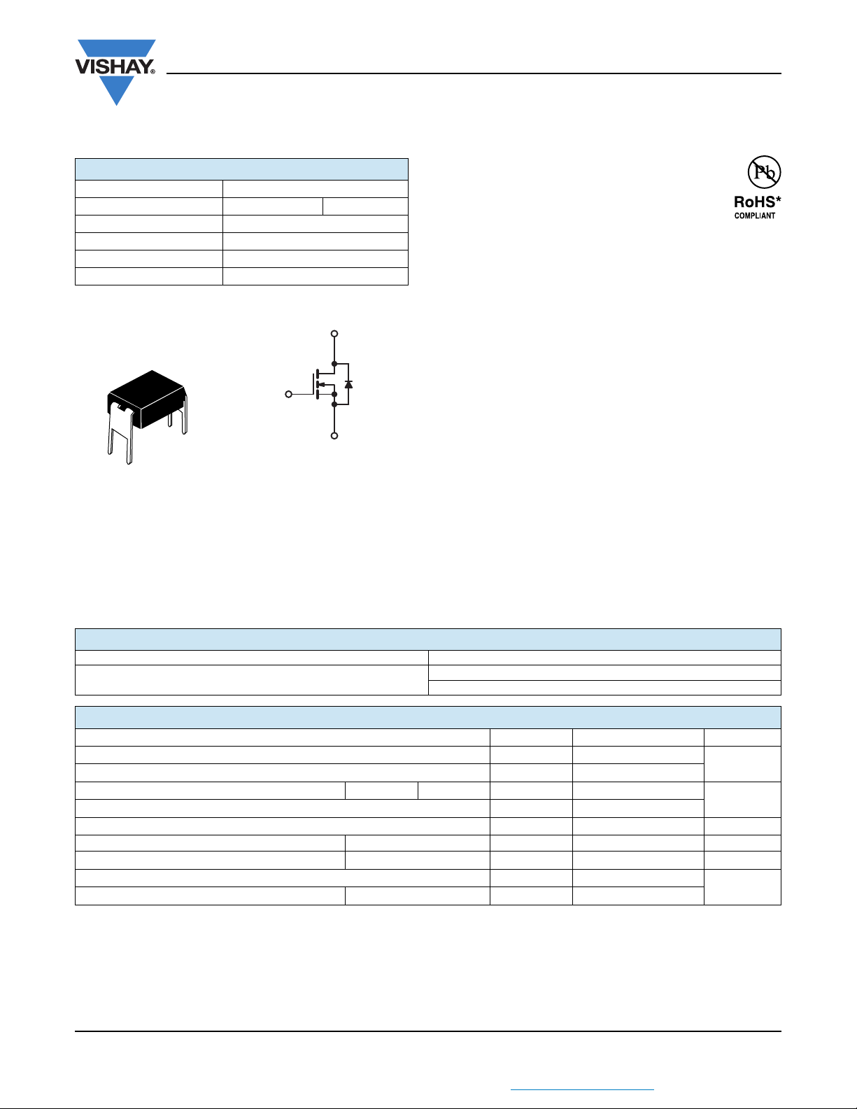
Power MOSFET
PRODUCT SUMMARY
VDS (V) 60
R
(Ω)V
DS(on)
Q
(Max.) (nC) 7
g
Q
(nC) 2
gs
Q
(nC) 7
gd
Configuration Single
= 10 V 0.8
GS
G
N-Channel MOSFET
FEATURES
• For Automatic Insertion
• Compact Plastic Package
•End Stackable
• Fast Switching
• Low Drive Current
• Easily Paralleled
• Excellent Temperature Stability
D
• Compliant to RoHS Directive 2002/95/EC
Note
* Pb containing terminations are not RoHS compliant, exemptions
may apply
DESCRIPTION
The HVMDIP technology is the key to Vishay’s advanced
line of power MOSFET transistors. The efficient geometry
and unique processing of the HVMDIP design achieves
S
very low on-state resistance combined with high
transconductance and extreme device ruggedness.
HVMDIPs feature all of the established advantages of
MOSFETs such as voltage control, very fast switching, ease
of paralleling, and temperature stability of the electrical
parameters.
The HVMDIP 4 pin, dual-in-line package brings the
advantages of HVMDIPs to high volume applications where
automatic PC board insertion is desireable, such as circuit
boards for computers, printers, telecommunications
equipment, and consumer products. Their compatibility with
automatic insertion equipment, low-profile and end
stackable features represent the stat-of-the-art in power
device packaging.
ORDERING INFORMATION
Package HVMDIP
Lead (Pb)-free
IRFD113PbF
SiHFD113-E3
ABSOLUTE MAXIMUM RATINGS (TC = 25 °C, unless otherwise noted)
PARAMETER SYMBOL LIMIT UNIT
Drain-Source Voltage
Gate-Source Voltage V
Continuous Drain Current V
Pulsed Drain Current
Linear Derating Factor 0.008 W/°C
Inductive Current, Clamped L = 100 μH I
Maximum Power Dissipation T
Operating Junction and Storage Temperature Range T
Soldering Recommendations (Peak Temperature) for 10 s 300
Notes
a. T
= 25 °C to 150 °C
J
b. Repetitive rating; pulse width limited by maximum junction temperature.
c. 1.6 mm from case.
S11-2479-Rev. A, 19-Dec-11
a
at 10 V TC = 25 °C I
b
GS
= 25 °C P
C
1
V
DS
± 20
GS
D
IDM 6.4
LM
D
, T
J
stg
- 55 to + 150
60
0.8
6.4 A
1.0 W
c
Document Number: 91487
V
A
°C
THIS DOCUMENT IS SUBJECT TO CHANGE WITHOUT NOTICE. THE PRODUCTS DESCRIBED HEREIN AND THIS DOCUMENT
ARE SUBJECT TO SPECIFIC DISCLAIMERS, SET FORTH AT www.vishay.com/doc?91000

IRFD113, SiHFD113
www.vishay.com
THERMAL RESISTANCE RATINGS
PARAMETER SYMBOL TYP. MAX. UNIT
Maximum Junction-to-Ambient R
thJA
- 120 °C/W
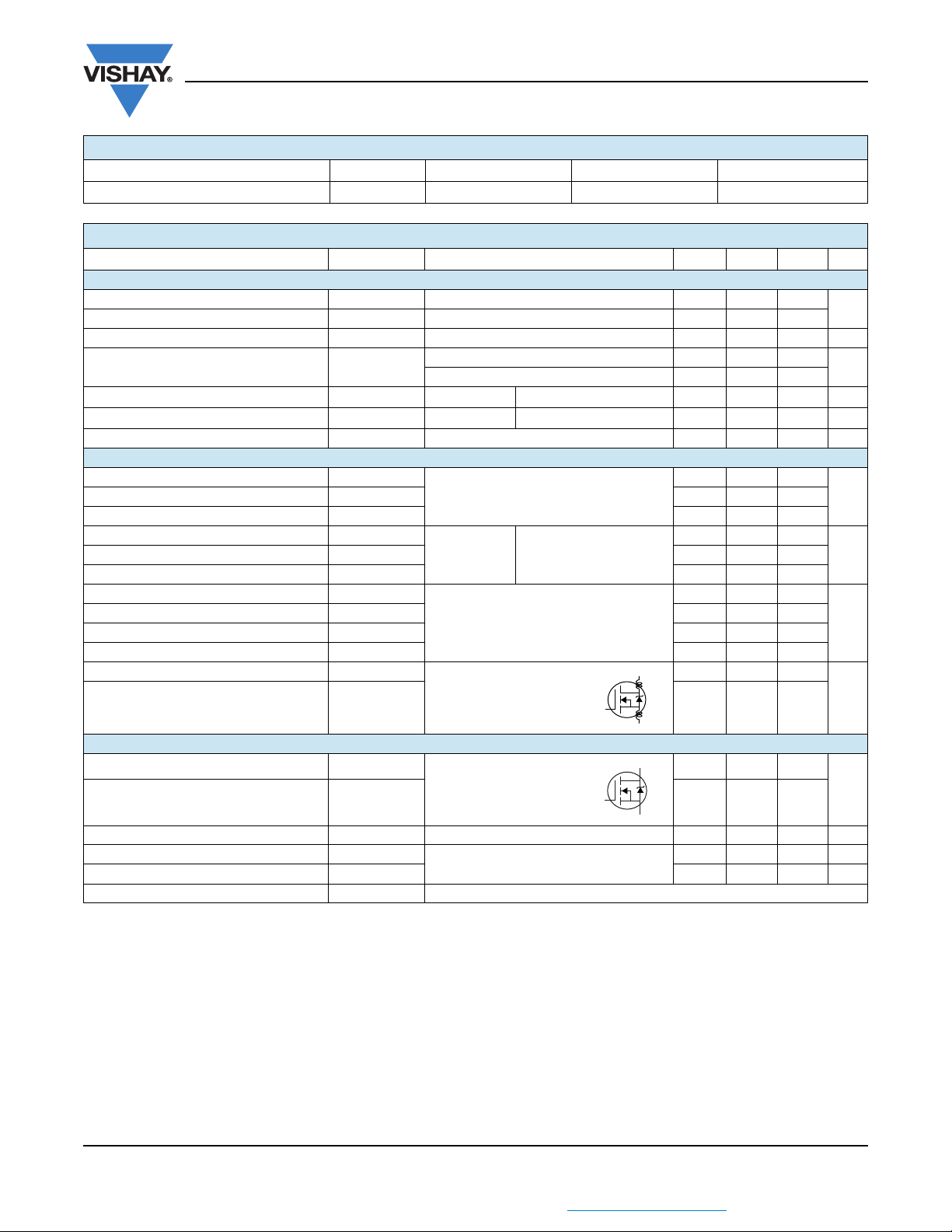
SPECIFICATIONS (TC = 25 °C, unless otherwise noted)
PARAMETER SYMBOL TEST CONDITIONS MIN. TYP. MAX. UNIT
Static
Drain-Source Breakdown Voltage V
Gate-Source Threshold Voltage V
Gate-Source Leakage I
Zero Gate Voltage Drain Current I
On-State Drain Current
Drain-Source On-State Resistance
Forward Transconductance
b
b
R
b
DS
GS(th)
V
GSS
DSS
I
D(on)
DS(on)
g
fs
VDS = max. rating x 0.8, VGS = 0 V, TC = 125 °C
V
VGS = 10 V ID = 0.8 A - 0.6 0.8 Ω
Dynamic
Input Capacitance C
Reverse Transfer Capacitance C
Total Gate Charge Q
Gate-Drain Charge Q
Turn-On Delay Time t
Rise Time t
Turn-Off Delay Time t
Fall Time t
Internal Drain Inductance L
Internal Source Inductance L
iss
-80100
oss
-2025
rss
g
-2-
gs
-7-
gd
d(on)
r
-1525
d(off)
-1020
f
D
S
Between lead,
2 mm (0.08") from
package and center of
die contact
Drain-Source Body Diode Characteristics
Continuous Source-Drain Diode Current I
Pulsed Diode Forward Current I
Body Diode Voltage
a
Body Diode Reverse Recovery Time t
Body Diode Reverse Recovery Charge Q
Forward Turn-On Time t
S
SM
V
SD
rr
rr
on
MOSFET symbol
showing the
integral reverse
p - n junction diode
TJ = 150 °C, IF = 1.0 A, dI/dt = 100 A/μs
Notes
a. Repetitive rating; pulse width limited by maximum junction temperature (see fig. 11).
b. Pulse width ≤ 300 μs; duty cycle ≤ 2 %.
VGS = 0 V, ID = 250 μA 60 - -
VDS = VGS, ID = 250 μA 2.0 - 4.0
= ± 20 V - - ± 500 nA
GS
VDS = max. rating, VGS = 0 V - - 250
= 10 V VDS > I
GS
VDS > I
D(on)
x R
DS(on)
D(on)
x R
max. 0.8 - - A
DS(on)
max., ID = 0.8 A 0.8 1.2 - S
VGS = 0 V,
V
= 25 V,
DS
f = 1.0 MHz
= 4 A,
I
V
GS
= 10 V
V
= 0.5 VDS , ID = 0.8 A,
DD
R
D
V
= 0.8 max. rating
DS
= 50 Ω
g
D
G
S
D
G
S
TA = 25 °C, IS = 0.8 A, VGS = 0 V - - 2 V
Intrinsic turn-on time is negligible (turn-on is dominated by LS and LD)
Vishay Siliconix
- - 1000
- 135 200
-57
-1020
-1525
-4.0-
-6.0-
--0.8
--6.4
- 100 - ns
-0.2-μC
V
μA
pFOutput Capacitance C
nC Gate-Source Charge Q
ns
nH
A
S11-2479-Rev. A, 19-Dec-11
2
Document Number: 91487
THIS DOCUMENT IS SUBJECT TO CHANGE WITHOUT NOTICE. THE PRODUCTS DESCRIBED HEREIN AND THIS DOCUMENT
ARE SUBJECT TO SPECIFIC DISCLAIMERS, SET FORTH AT www.vishay.com/doc?91000

www.vishay.com
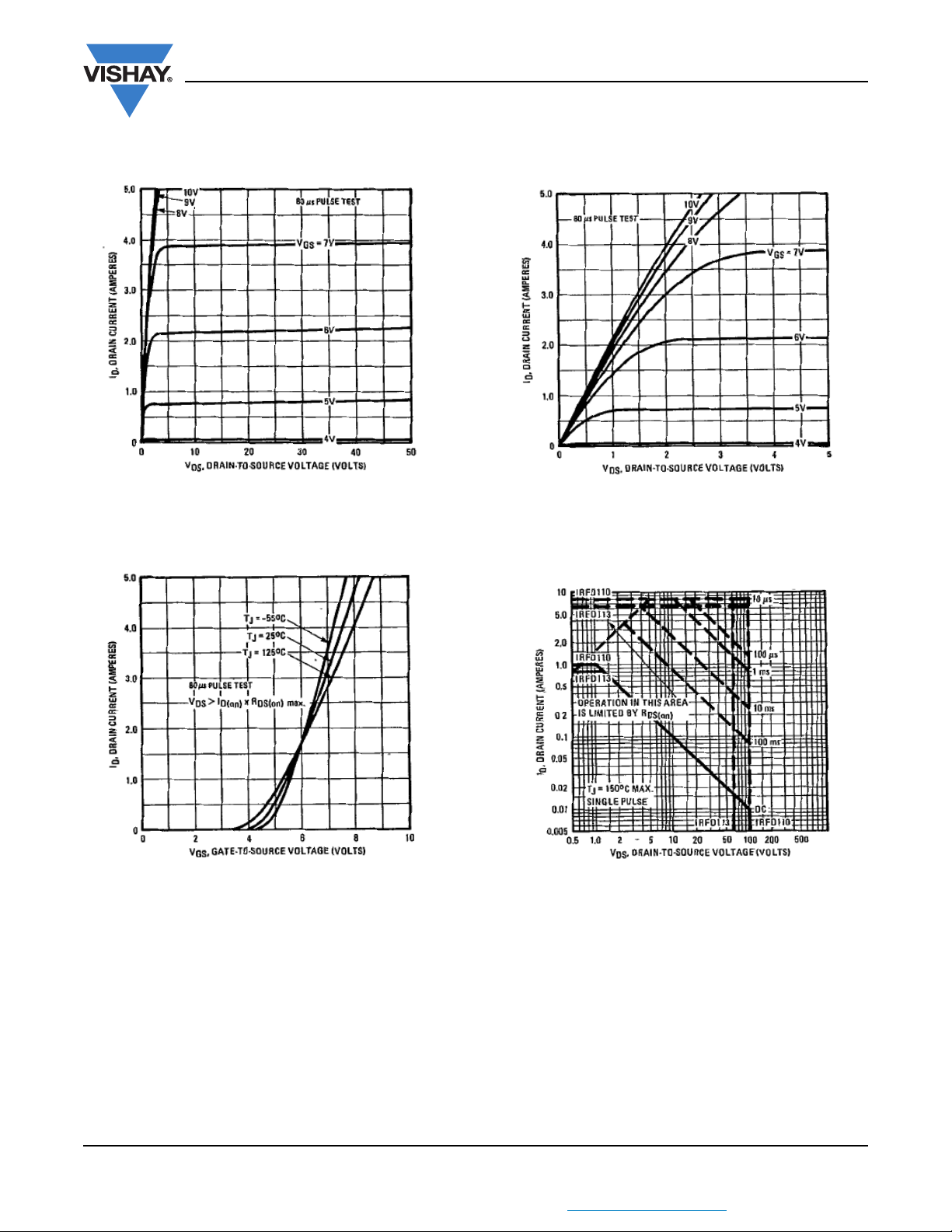
TYPICAL CHARACTERISTICS (25 °C, unless otherwise noted)
IRFD113, SiHFD113
Vishay Siliconix
Fig. 1 - Typical Output Characteristics
Fig. 2 - Typical Transfer Characteristics
Fig. 3 - Typical Saturation Characteristics
Fig. 4 - Maximum Safe Operatung Area
S11-2479-Rev. A, 19-Dec-11
THIS DOCUMENT IS SUBJECT TO CHANGE WITHOUT NOTICE. THE PRODUCTS DESCRIBED HEREIN AND THIS DOCUMENT
ARE SUBJECT TO SPECIFIC DISCLAIMERS, SET FORTH AT www.vishay.com/doc?91000
3
Document Number: 91487
 Loading...