

P-Channel 20-V (D-S) MOSFET
20
Conti
t (TJ = 150_C)
a
I
A
b
C/W
Si8401DB
Vishay Siliconix
PRODUCT SUMMARY
V
(V) r
DS
−
−
DS(on)
0.065 @ VGS = −4.5 V
0.095 @ VGS = −2.5 V −4.1
(W) I
D
−4.9
(A)
FEATURES
D TrenchFETr Power MOSFET
D New MICRO FOOTr Chipscale Packaging
Reduces Footprint Area Profile (0.62 mm) and
On-Resistance Per Footprint Area
D Pin Compatible to Industry Standard Si3443DV
APPLICATIONS
D PA, Battery and Load Switch
D Battery Charger Switch
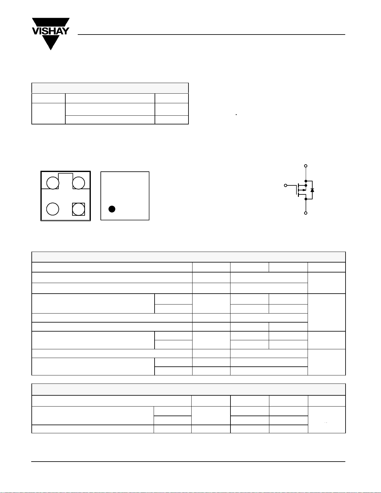
MICRO FOOT
Bump Side View Backside View
32
DD
8401
xxx
S
41
G
Device Marking: 8401
Ordering Information: Si8401DB-T1
D PA Switch
xxx = Date/Lot Traceability Code
Si8401DB-T1—E1 (Lead (Pb)-Free)
ABSOLUTE MAXIMUM RATINGS (TA = 25_C UNLESS OTHERWISE NOTED)
Parameter Symbol 5 secs Steady State Unit
Drain-Source Voltage V
Gate-Source Voltage V
a
=
nuous Drain Curren
Pulsed Drain Current I
continuous Source Current (Diode Conduction)
Maximum Power Dissipation
Operating Junction and Storage Temperature Range TJ, T
Package Reflow Conditions
_
a
a
TA = 25_C
TA = 70_C
TA = 25_C
TA = 70_C
VPR 215/245
IR/Convection 220/250
P
DM
I
DS
GS
D
S
D
stg
−4.9
−3.9 −2.8
−2.5 −2.5
2.77 1.47
1.77 0.94
−20
"12
−10
−55 to 150 _C
c
c
S
G
D
P-Channel MOSFET
−3.6
_
_C
V
W
THERMAL RESISTANCE RATINGS
Parameter Symbol Typical Maximum Unit
Maximum Junction-to-Ambient
Maximum Junction-to-Foot (drain) Steady State R
Notes
a. Surface Mounted on 1” x 1” FR4 Board.
b. Refer to IPC/JEDEC (J-STD-020A), no manual or hand soldering.
c. Package reflow conditions for lead-free.
Document Number: 71674
S-50066—Rev. G, 17-Jan-05
a
t v 5 sec
Steady State
R
thJA
thJF
35 45
72 85
16 20
_C/W
www.vishay.com
1
Si8401DB
DS
,
GS
,
D
VDD = −10 V, RL = 10 W
ns
Vishay Siliconix
SPECIFICATIONS (TJ = 25_C UNLESS OTHERWISE NOTED)
Parameter Symbol T est Condition Min Typ Max Unit
Static
Gate Threshold Voltage V
Gate-Body Leakage I
Zero Gate Voltage Drain Current I
On-State Drain Current
Drain-Source On-State Resistance
Forward Transconductance
Diode Forward Voltage
Dynamic
b
a
a
a
a
Total Gate Charge Q
Gate-Source Charge Q
Gate-Drain Charge Q
Turn-On Delay Time t
Rise Time t
Turn-Off Delay Time t
Fall Time t
Source-Drain Reverse Recovery Time t
Reverse Recovery Charge Q
Notes
a. Pulse test; pulse width v 300 ms, duty cycle v 2%.
b. Guaranteed by design, not subject to production testing.
Stresses beyond those listed under “Absolute Maximum Ratings” may cause permanent damage to the device. These are stress ratings only, and functional operation
of the device at these or any other conditions beyond those indicated in the operational sections of the specifications is not implied. Exposure to absolute maximum rating
GS(th)
GSS
DSS
I
D(on)
r
DS(on)
g
V
d(on)
d(off)
fs
SD
g
gs
gd
r
f
rr
rr
VDS = VGS, I
= −250 mA −0.45 −0.9 1.4 V
D
VDS = 0 V, VGS = "12 V "100 nA
VDS = −20 V, VGS = 0 V −1
VDS = −20 V, VGS = 0 V, TJ = 70_C −5
VDS v −5 V, VGS = −4.5 V −5 A
VGS = −4.5 V, ID = −1 A 0.057 0.065
VGS = −2.5 V, ID = −1 A 0.080 0.095
VDS = −10 V, ID = −1 A
6 S
IS = −1 A, VGS = 0 V −0.73 −1.1 V
11 17
V
= −10 V, VGS = −4.5 V, ID = −1 A 2.1 nC
DS
2.9
17 25
VDD = −10 V, RL = 10 W
ID ^ −1 A, V
GEN
= −4.5 V, RG = 6 W
28 45
88 135
60 90
IF = −1 A, di/dt = 100 A/ms
40 60
20 30 nC
mA
W
ns
conditions for extended periods may affect device reliability.
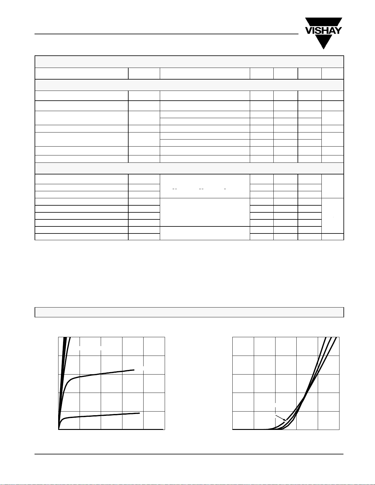
TYPICAL CHARACTERISTICS (25_C UNLESS NOTED)
10
8
6
4
− Drain Current (A)I
D
2
0
0246810
www.vishay.com
2
Output Characteristics Transfer Characteristics
VGS = 5 thru 2.5 V
2 V
1.5 V
VDS − Drain-to-Source Voltage (V)
10
8
6
4
− Drain Current (A)I
D
2
TC = 125_C
25_C
−55_C
0
0.0 0.5 1.0 1.5 2.0 2.5
VGS − Gate-to-Source Voltage (V)
Document Number: 71674
S-50066—Rev. G, 17-Jan-05
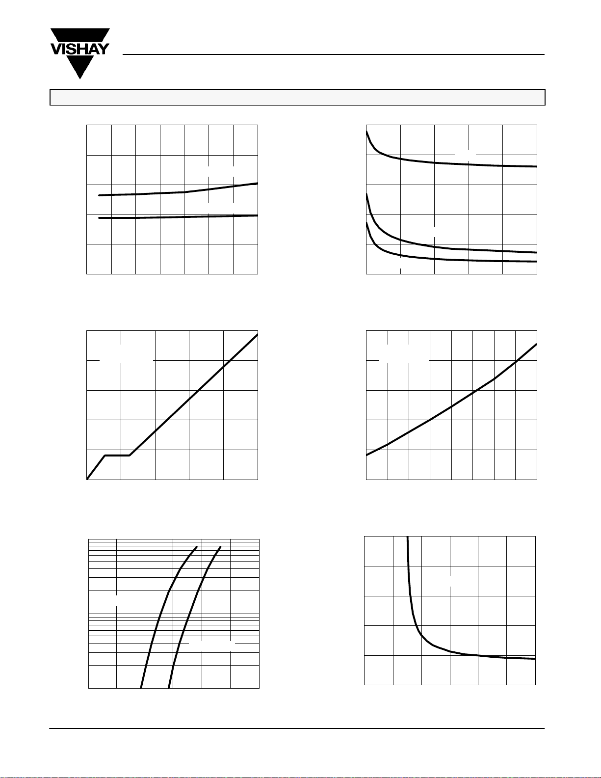
TYPICAL CHARACTERISTICS (25_C UNLESS NOTED)
Si8401DB
Vishay Siliconix
W )
− On-Resistance (r
DS(on)
0.15
On-Resistance vs. Drain Current
0.12
VGS = 2.5 V
0.09
0.06
0.03
0.00
01234567
ID − Drain Current (A)
10
VDS = 10 V
I
= 1 A
D
8
6
Gate Charge
VGS = 4.5 V
1500
1200
900
600
C − Capacitance (pF)
300
C
0
1.6
1.4
1.2
rss
048121620
V
On-Resistance vs. Junction Temperature
VGS = 4.5 V
I
= 1 A
D
Capacitance
C
iss
C
oss
− Drain-to-Source Voltage (V)
DS
− Gate-to-Source Voltage (V)
GS
V
− Source Current (A)I
S
0.1
4
2
0
048121620
Qg − Total Gate Charge (nC)
Source-Drain Diode Forward Voltage On-Resistance vs. Gate-to-Source Voltage
10
TJ = 150_C
1
TJ = 25_C
0.0 0.2 0.4 0.6 0.8 1.0 1.2
VSD − Source-to-Drain Voltage (V)
1.0
− On-Resiistance
(Normalized)
DS(on)
r
0.8
0.6
−50 −25 0 25 50 75 100 125 150
T
− Junction Temperature (_C)
J
0.30
0.24
W )
0.18
0.12
− On-Resistance (r
0.06
DS(on)
0.00
0123456
VGS − Gate-to-Source Voltage (V)
ID = 1 A
Document Number: 71674
S-50066—Rev. G, 17-Jan-05
www.vishay.com
3

Si8401DB
Vishay Siliconix
TYPICAL CHARACTERISTICS (25_C UNLESS NOTED)
0.4
0.3
ID = 250 mA
0.2
0.1
Variance (V)V
GS(th)
0.0
−0.1
−0.2
−50 −25 0 25 50 75 100 125 150
TJ − Temperature (_C)
Normalized Thermal Transient Impedance, Junction-to-Ambient
2
1
Duty Cycle = 0.5
0.2
0.1
0.1
Threshold Voltage
0.01
0.05
0.02
Single Pulse
−4
10
−3
10
Thermal Impedance
Normalized Effective Transient
Single Pulse Power, Juncion-T o-Ambient
80
60
40
Power (W)
20
0
0.001
0.01 0.1 1
Time (sec)
Notes:
P
DM
t
1
t
2
t
thJA
t
thJA
100
1
2
= 72_C/W
(t)
1. Duty Cycle, D =
2. Per Unit Base = R
3. TJM − TA = PDMZ
4. Surface Mounted
−2
10
−1
1 10 60010
Square Wave Pulse Duration (sec)
10
2
1
0.1
Thermal Impedance
Normalized Effective Transient
0.01
www.vishay.com
4
Duty Cycle = 0.5
0.2
0.1
0.05
0.02
−4
10
Single Pulse
Normalized Thermal Transient Impedance, Junction-to-Foot
−3
10
−2
10
−1
Square Wave Pulse Duration (sec)
1
1010
Document Number: 71674
S-50066—Rev. G, 17-Jan-05

PACKAGE OUTLINE
MICRO FOOT: 4-BUMP (2 X 2, 0.8-mm PITCH)
4 O 0.30 X 0.31
Note 3
Solder Mask O X 0.40
e
b Diamerter
e
Recommended Land
Si8401DB
Vishay Siliconix
A
2
A
A
1
Silicon
Bump Note 2
S
E
8401
XXX
Mark on Backside of Die
NOTES (Unless Otherwise Specified):
1. Laser mark on the silicon die back, coated with a thin metal.
2. Bumps are Eutectic solder 63/57 Sn/Pb. (Sn 3.8 Ag, 0.7 Cu for Pb-free bumps)
3. Non-solder mask defined copper landing pad.
4. The flat side of wafers is oriented at the bottom.
MILLIMETERS* INCHES
Dim Min Max Min Max
A
A
1
A
2
b
D
E
e
S
0.600 0.650 0.0236 0.0256
0.260 0.290 0.0102 0.0114
0.340 0.360 0.0134 0.0142
0.370 0.410 0.0146 0.0161
1.520 1.600 0.0598 0.0630
1.520 1.600 0.0598 0.0630
0.750 0.850 0.0295 0.0335
0.370 0.380 0.0146 0.0150
e
e S
D
* Use millimeters as the primary measurement.
Vishay Siliconix maintains worldwide manufacturing capability. Products m ay be manufac tured at one of several qualified locations. Reliability d at a for Silicon Technology and
Package Reliability represent a composite of all qualified locations. For related documents such as package/tape drawings, part marking, and reliability data, see
http://www.vishay.com/ppg?71674.
Document Number: 71674
S-50066—Rev. G, 17-Jan-05
www.vishay.com
5

Legal Disclaimer Notice
Vishay
Notice
Specifications of the products displayed herein are subject to change without notice. Vishay Intertechnology, Inc.,
or anyone on its behalf, assumes no responsibility or liability for any errors or inaccuracies.
Information contained herein is intended to provide a product description only. No license, express or implied, by
estoppel or otherwise, to any intellectual property rights is granted by this document. Except as provided in Vishay's
terms and conditions of sale for such products, Vishay assumes no liability whatsoever, and disclaims any express
or implied warranty, relating to sale and/or use of Vishay products including liability or warranties relating to fitness
for a particular purpose, merchantability, or infringement of any patent, copyright, or other intellectual property right.
The products shown herein are not designed for use in medical, life-saving, or life-sustaining applications.
Customers using or selling these products for use in such applications do so at their own risk and agree to fully
indemnify Vishay for any damages resulting from such improper use or sale.
Document Number: 91000 www.vishay.com
Revision: 08-Apr-05 1

 Loading...