

30
Conti
t (TJ = 150_C)
a
I
A
C/W
查询SI7991DP供应商
Si7991DP
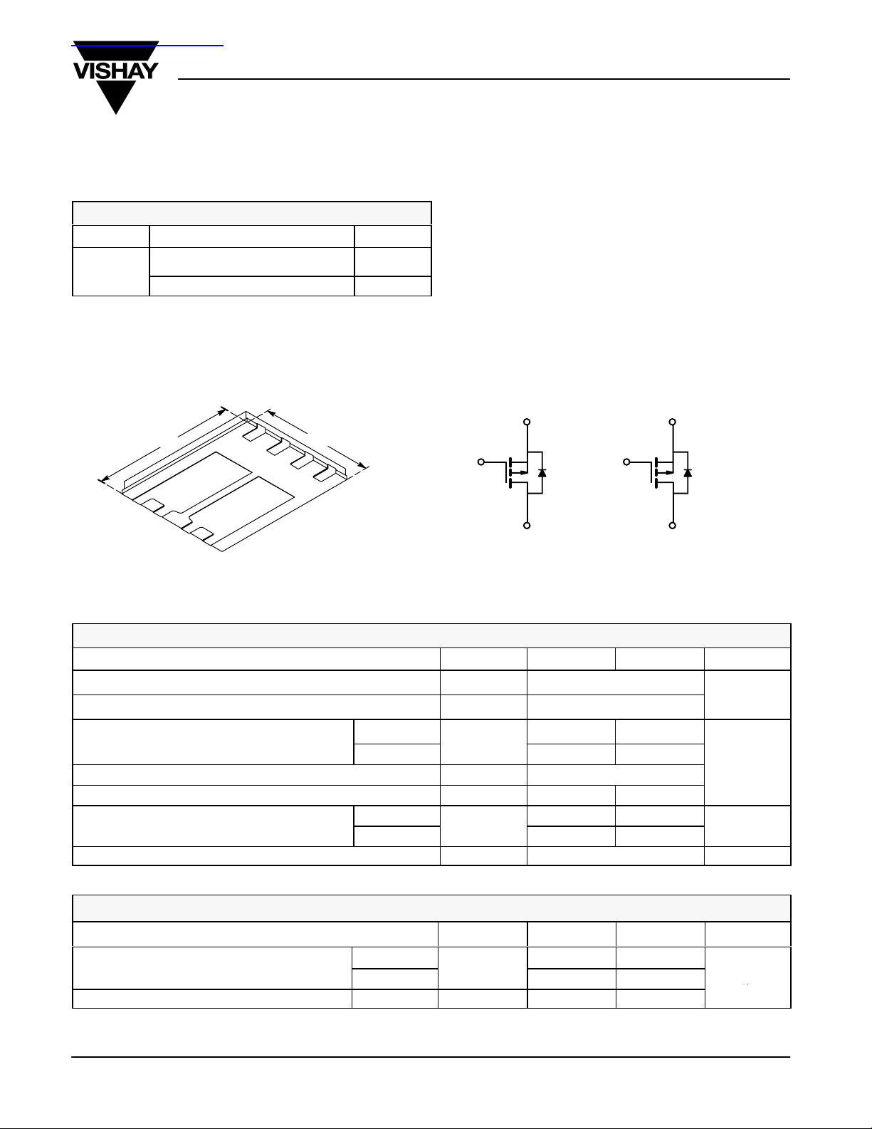
PRODUCT SUMMARY
V
(V) r
DS
−
−
6.15 mm
D1
8
D1
7
6
DS(on)
0.023 @ VGS = −10 V
0.035 @ VGS = −4.5 V −8.1
PowerPAK SO-8
D2
D2
5
Bottom View
New Product
Dual P-Channel 30-V (D-S) MOSFET
FEATURES
D TrenchFETr Power MOSFET
(W) I
S1
1
5.15 mm
G1
2
S2
3
G2
4
Ordering Information: Si7991DP-T1
(A)
D
−10.2
D New Low Thermal Resistance PowerPAKr Package
with Low 1.07-mm Profile
APPLICATIONS
D Load Switch
− Notebook PCs
− Desktop PCs
− Game Stations
D Battery Switch
S
1
G
1
P-Channel MOSFET
D
1
G
2
Vishay Siliconix
S
2
D
2
P-Channel MOSFET
ABSOLUTE MAXIMUM RATINGS (TA = 25_C UNLESS OTHERWISE NOTED)
Parameter Symbol 10 secs Steady State Unit
Drain-Source Voltage V
Gate-Source Voltage V
a
=
nuous Drain Curren
Pulsed Drain Current I
continuous Source Current (Diode Conduction)
Maximum Power Dissipation
Operating Junction and Storage Temperature Range TJ, T
_
a
a
TA = 25_C
TA = 70_C
TA = 25_C
TA = 70_C
P
DM
I
GS
DS
D
S
D
stg
−10.2
−8.2 −5.3
−2.9 −1.2
3.5 1.4
2.2 0.9
−30
"20
−30
−55 to 150 _C
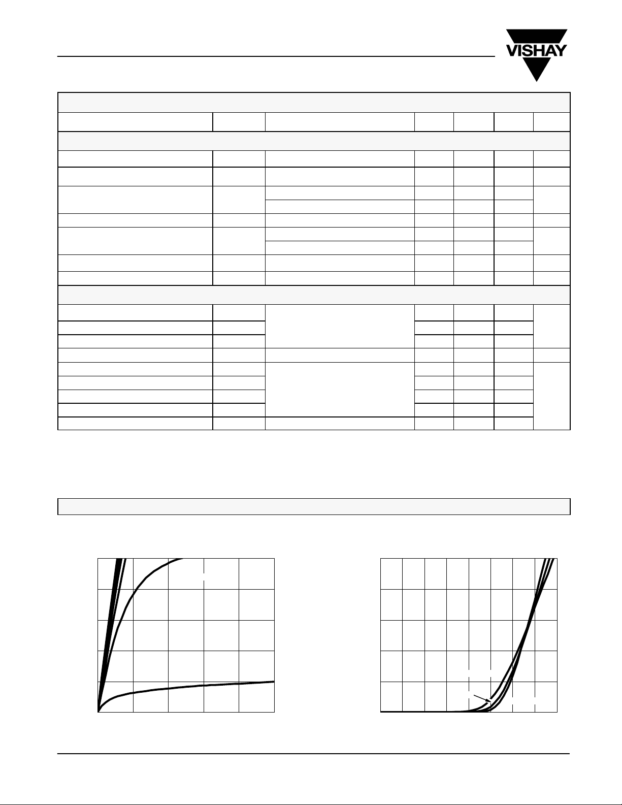
THERMAL RESISTANCE RATINGS
Parameter Symbol Typical Maximum Unit
Maximum Junction-to-Ambient
Maximum Junction-to-Case (Drain) Steady State R
Notes
a. Surface Mounted on 1” x 1” FR4 Board.
a
t v 10 sec
Steady State
R
thJA
thJC
28 35
60 85
3 3.7
V
−6.6
W
_C/W
Document Number: 72515
S-32127—Rev. B, 27-Oct-03
www.vishay.com
1
Si7991DP
VDD = −15 V, RL = 15 W
Vishay Siliconix
New Product
SPECIFICATIONS (TJ = 25_C UNLESS OTHERWISE NOTED)
Parameter Symbol Test Condition Min Typ Max Unit
Static
Gate Threshold Voltage V
Gate-Body Leakage I
Zero Gate Voltage Drain Current I
On-State Drain Current
Drain-Source On-State Resistance
Forward Transconductance
Diode Forward Voltage
Dynamic
Total Gate Charge Q
Gate-Source Charge Q
Gate-Drain Charge Q
Gate Resistance R
Turn-On Delay Time t
Rise Time t
Turn-Off Delay Time t
Fall Time t
Source-Drain Reverse Recovery Time t
Notes
a. Pulse test; pulse width v 300 ms, duty cycle v 2%.
b. Guaranteed by design, not subject to production testing.
b
a
a
a
a
GS(th)
GSS
DSS
I
D(on)
r
DS(on)
g
V
d(on)
d(off)
fs
SD
gs
gd
r
f
rr
g
g
VDS = VGS, I
VDS = 0 V, VGS = "20 V "100 nA
VDS = −30 V, VGS = 0 V −1
VDS = −30 V, VGS = 0 V, TJ = 55_C −5
VDS v −5 V, VGS = −10 V −30 A
VGS = −10 V, ID = −10.0 A 0.019 0.023
VGS = −4.5 V, ID = −8.2 A 0.027 0.035
VDS = −15 V, ID = −10.0 A
IS = −2.9 A, VGS = 0 V −0.8 −1.2 V
V
= −15 V, VGS = −10 V, ID = −10.0 A 6.3 nC
DS
VDD = −15 V, RL = 15 W
ID ^ −1 A, V
IF = −2.9 A, di/dt = 100 A/ms 45 70
= −250 mA −1 −3 V
D
f = 1 MHz 10 W
= −10 V, RG = 6 W
GEN
22 S
38 57
9.7
10 15
15 25
130 200
70 105
mA
W
ns
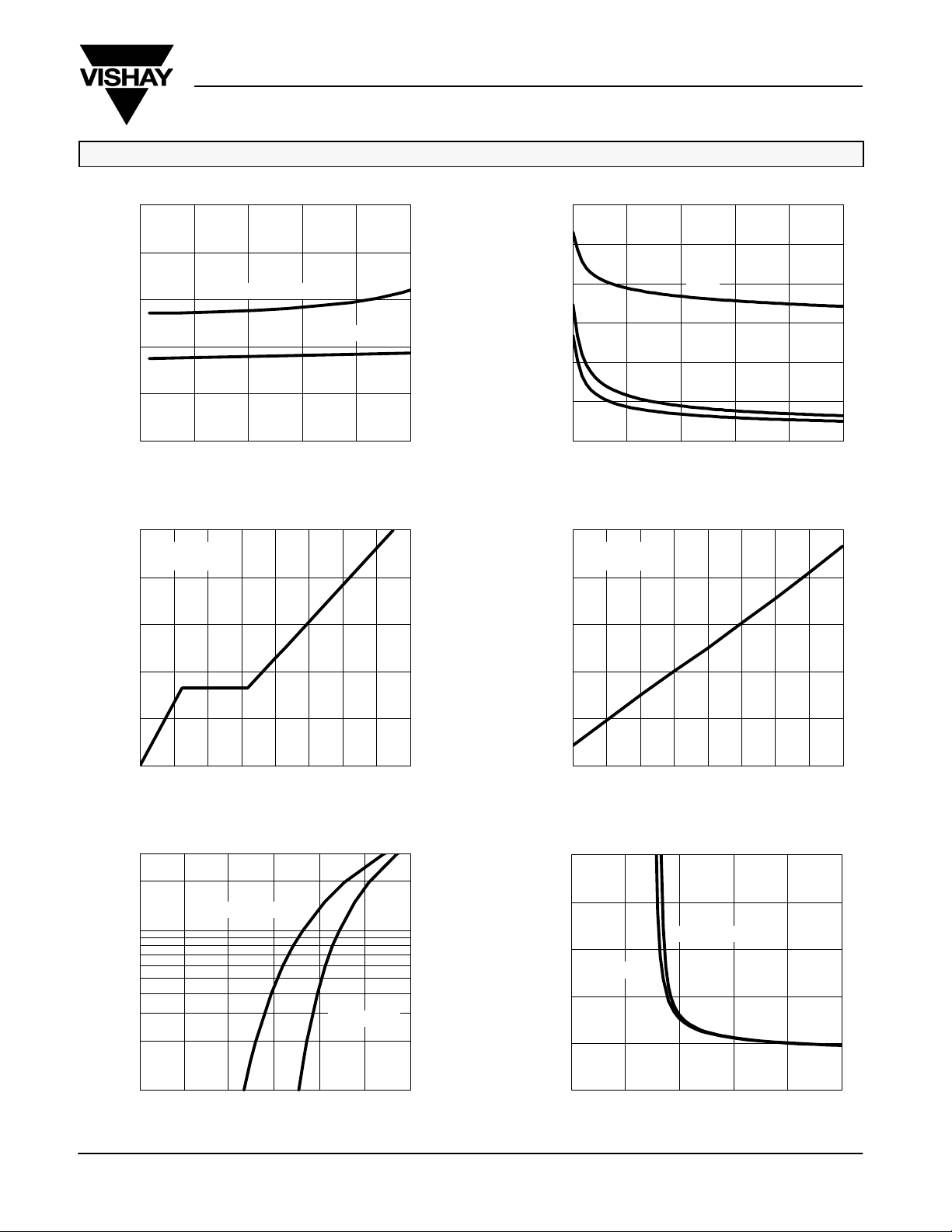
TYPICAL CHARACTERISTICS (25_C UNLESS NOTED)
30
24
18
12
− Drain Current (A)I
D
6
0
012345
www.vishay.com
2
Output Characteristics Transfer Characteristics
VGS = 10 thru 4 V
3 V
VDS − Drain-to-Source Voltage (V)
30
24
18
12
− Drain Current (A)I
D
6
0
0.0 0.5 1.0 1.5 2.0 2.5 3.0 3.5 4.0
VGS − Gate-to-Source Voltage (V)
TC = 125_C
25_C
Document Number: 72515
S-32127—Rev. B, 27-Oct-03
−55_C
Si7991DP
New Product
TYPICAL CHARACTERISTICS (25_C UNLESS NOTED)
On-Resistance vs. Drain Current
0.05
W )
0.04
VGS = 4.5 V
− Drain Current (A)
I
D
Gate Charge
VGS = 10 V
− On-Resistance (r
DS(on)
0.03
0.02
0.01
0.00
0 6 12 18 24 30
10
VDS = 15 V
I
= 10 A
D
8
3000
2500
2000
1500
C − Capacitance (pF)
1000
500
C
0
0 6 12 18 24 30
On-Resistance vs. Junction Temperature
1.6
VGS = 10 V
W)
I
1.4
Vishay Siliconix
Capacitance
C
iss
C
oss
rss
VDS − Drain-to-Source Voltage (V)
= 10 A
D
− Gate-to-Source Voltage (V)
GS
V
− Source Current (A)I
S
6
4
2
0
0 5 10 15 20 25 30 35 40
Qg − Total Gate Charge (nC)
Source-Drain Diode Forward Voltage On-Resistance vs. Gate-to-Source Voltage
30
TJ = 150_C
10
TJ = 25_C
1.2
(Normalized)
− On-Resistance (r
1.0
DS(on)
0.8
0.6
−50 −25 0 25 50 75 100 125 150
T
− Junction Temperature (_C)
J
0.10
0.08
W )
ID = 10 A
− On-Resistance (r
DS(on)
0.06
ID = 5 A
0.04
0.02
1
0.0 0.2 0.4 0.6 0.8 1.0 1.2
VSD − Source-to-Drain Voltage (V) VGS − Gate-to-Source Voltage (V)
Document Number: 72515
S-32127—Rev. B, 27-Oct-03
0.00
0246810
www.vishay.com
3

Si7991DP
Vishay Siliconix
New Product
TYPICAL CHARACTERISTICS (25_C UNLESS NOTED)
Threshold Voltage
0.8
0.6
ID = 250 mA
0.4
0.2
Variance (V)V
GS(th)
0.0
−0.2
−0.4
−50 −25 0 25 50 75 100 125 150
TJ − Temperature (_C)
100
r
DS(on)
Safe Operating Area
Limited
30
24
18
Power (W)
12
6
0
I
Limited
DM
Single Pulse Power, Junction-to-Ambient
0.1 100010.010.001 10 100
Time (sec)
2
1
0.1
Thermal Impedance
Normalized Effective Transient
0.01
10
Duty Cycle = 0.5
0.2
0.1
0.05
0.02
Single Pulse
−4
10
P(t) = 0.001
I
D(on)
1
Limited
P(t) = 0.01
P(t) = 0.1
− Drain Current (A)I
D
0.1
TA = 25_C
Single Pulse
P(t) = 1
P(t) = 10
dc
BV
Limited
0.01
DSS
0.1 1 10 100
VDS − Drain-to-Source Voltage (V)
Normalized Thermal Transient Impedance, Junction-to-Ambient
Notes:
P
DM
t
1
t
2
t
thJA
t
thJA
100
1
2
= 60_C/W
(t)
1. Duty Cycle, D =
2. Per Unit Base = R
3. TJM − TA = PDMZ
4. Surface Mounted
−3
10
−2
10
−1
1 10 60010
Square Wave Pulse Duration (sec)
www.vishay.com
4
Document Number: 72515
S-32127—Rev. B, 27-Oct-03

Si7991DP
New Product
TYPICAL CHARACTERISTICS (25_C UNLESS NOTED)
Normalized Thermal Transient Impedance, Junction-to-Case
2
1
Duty Cycle = 0.5
0.2
0.1
0.1
Thermal Impedance
Normalized Effective Transient
0.01
10
Single Pulse
−4
0.05
0.02
−3
10
Square Wave Pulse Duration (sec)
−2
10
Vishay Siliconix
−1
110
Document Number: 72515
S-32127—Rev. B, 27-Oct-03
www.vishay.com
5
 Loading...