

Si7403DN
C/W
PRODUCT SUMMARY
V
(V) r
DS
–20
3.30 mm
D
8
D
7
DS(on)
0.1 @ VGS = –4.5 V
0.135 @ VGS = –2.5 V –3.8
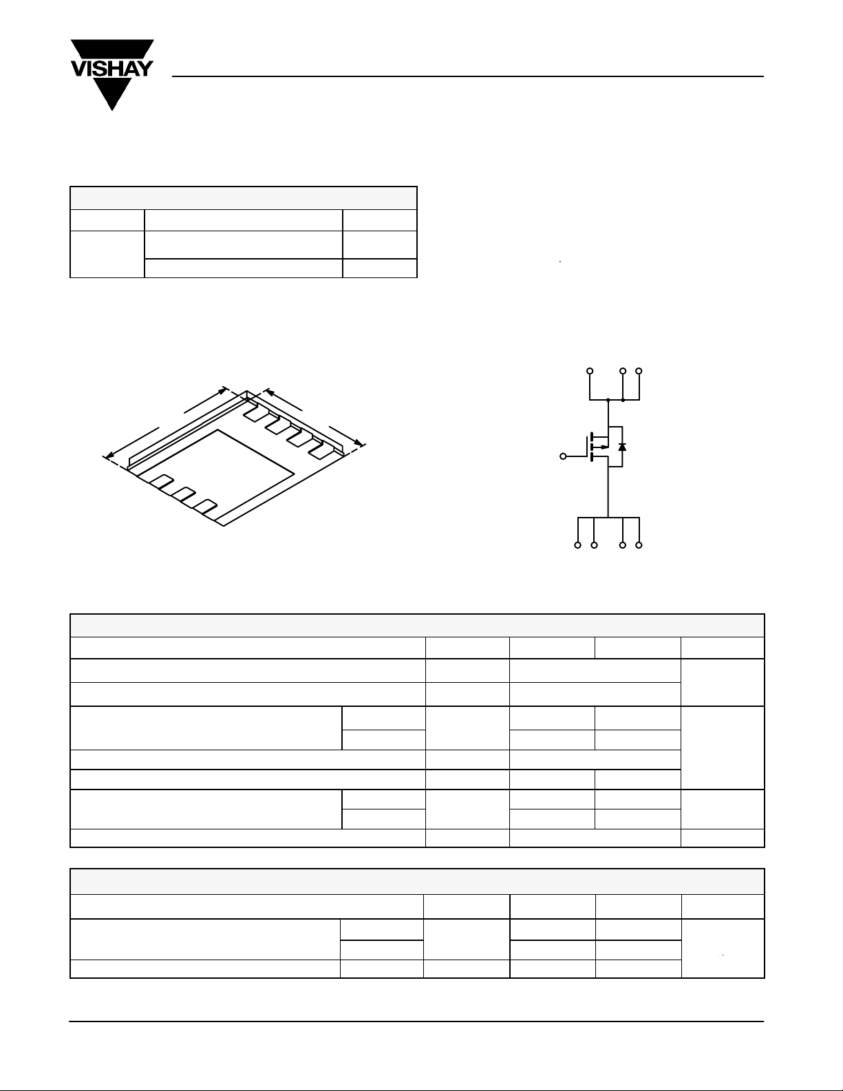
PowerPAKt 1212-8
D
6
D
5
New Product
P-Channel 20-V (D-S) MOSFET
FEATURES
(W) I
S
1
3.30 mm
S
2
S
3
G
4
D
–4.5
(A)
D TrenchFETr Power MOSFETS: 2.5-V Rated
D New PowerPAKt Package
– Low Thermal Resistance, R
– Low 1.07-mm Profile
APPLICATIONS
D Load Switching
D PA Switching
P-Channel MOSFET
Vishay Siliconix
thJC
SDDS S
G
Bottom View
DD
ABSOLUTE MAXIMUM RATINGS (TA = 25_C UNLESS OTHERWISE NOTED)
Parameter Symbol 10 secs Steady State Unit
Drain-Source Voltage V
Gate-Source Voltage V
a
a
Continuous Drain Current (TJ = 150_C)
Pulsed Drain Current I
continuous Source Current (Diode Conduction)
Maximum Power Dissipation
Operating Junction and Storage Temperature Range TJ, T
_
a
a
TA = 25_C
TA = 85_C
TA = 25_C 3.5 1.5
TA = 85_C
P
I
DM
I
DS
GS
D
S
D
stg
–4.5
–3.2 –2.1
–3.0 –1.3
1.9 0.8
–20
"8
–20
–55 to 150 _C
THERMAL RESISTANCE RATINGS
Parameter Symbol Typical Maximum Unit
Maximum Junction-to-Ambient
Maximum Junction-to-Case Steady State R
a
t v 10 sec 28 35
Steady State
R
thJA
thJC
65 81
4.5 5.6
V
–2.9
A
W
_C/W
Notes
a. Surface Mounted on 1” x 1” FR4 Board.
Document Number: 71431
S-03390—Rev. A, 02-Apr-01
www.vishay.com
1
Si7403DN
W
Vishay Siliconix
New Product
SPECIFICATIONS (TJ = 25_C UNLESS OTHERWISE NOTED)
Parameter Symbol Test Condition Min Typ Max Unit
Static
Gate Threshold Voltage V
Gate-Body Leakage I
Zero Gate Voltage Drain Current I
On-State Drain Current
Drain-Source On-State Resistance
Forward Transconductance
Diode Forward Voltage
Dynamic
Total Gate Charge Q
Gate-Source Charge Q
Gate-Drain Charge Q
Turn-On Delay Time t
Rise Time t
Turn-Off Delay Time t
Fall Time t
Source-Drain Reverse Recovery Time t
b
a
a
a
a
I
r
DS(on)
GS(th)
GSS
DSS
D(on)
g
fs
V
SD
g
gs
gd
d(on)
r
d(off)
f
rr
VDS = VGS, I
VDS = 0 V, VGS = "4.5 V
VDS = –20 V, VGS = 0 V –1
VDS = –20 V, VGS = 0 V, TJ = 70_C –5
VDS = –5 V, VGS = –4.5 V –10
VDS = –5 V, VGS = –2.5 V –4
VGS = –4.5 V, ID = –3.3 A 0.078 0.1
VGS = –2.5 V, ID = –2.9 A 0.110 0.135
VDS = –10 V, ID = –3.3 A 8.8 S
IS = –1.6 A, VGS = 0 V 0.8 –1.2 V
V
= –10 V, VGS = –4.5 V, ID = –4.5 A 1.5 nC
DS
VDD = –10 V, RL = 10 W
VDD = –10 V, RL = 10
ID ^ –1.6 A, V
IF = –1.6 A, di/dt = 100 A/ms 50 80
= –250 mA –0.45 V
D
= –4.5 V, RG = 6 W
GEN
"100 nA
8.6 14
3.1
27 50
17 30
52 80
45 70
mA
A
W
ns
Notes
a. Pulse test; pulse width v 300 ms, duty cycle v 2%.
b. Guaranteed by design, not subject to production testing.
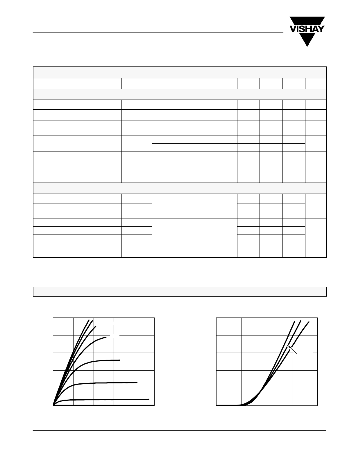
TYPICAL CHARACTERISTICS (25_C UNLESS NOTED)
20
16
12
8
– Drain Current (A)I
D
4
0
012345
Output Characteristics Transfer Characteristics
VGS = 4.5, 4, 3.5 V
3 V
2.5 V
2 V
1.5 V
VDS – Drain-to-Source Voltage (V)
20
TC = –55_C
16
125_C
12
8
– Drain Current (A)I
D
4
0
01234
VGS – Gate-to-Source Voltage (V)
25_C
www.vishay.com
2
Document Number: 71431
S-03390—Rev. A, 02-Apr-01

Si7403DN
New Product
TYPICAL CHARACTERISTICS (25_C UNLESS NOTED)
0.30
0.24
W )
0.18
0.12
– On-Resistance (r
DS(on)
0.06
0.00
5
4
3
2
– Gate-to-Source Voltage (V)
1
GS
V
On-Resistance vs. Drain Current
VGS = 2.5 V
VGS = 4.5 V
048121620
ID – Drain Current (A)
Gate Charge
VDS = 10 V
I
= 3.3 A
D
C – Capacitance (pF)
W )
(Normalized)
– On-Resistance (r
DS(on)
Vishay Siliconix
1400
1200
1000
800
600
400
200
C
0
1.8
1.6
1.4
1.2
1.0
0.8
rss
048121620
V
On-Resistance vs. Junction Temperature
VGS = 4.5 V
I
= 3.3 A
D
Capacitance
C
oss
– Drain-to-Source Voltage (V)
DS
C
iss
0
0246810
Qg – Total Gate Charge (nC)
Source-Drain Diode Forward Voltage On-Resistance vs. Gate-to-Source Voltage
20
10
TJ = 150_C
– Source Current (A)I
S
1
0 0.25 0.50 0.75 1.00 1.25 1.50
VSD – Source-to-Drain Voltage (V) VGS – Gate-to-Source Voltage (V)
Document Number: 71431
S-03390—Rev. A, 02-Apr-01
TJ = 25_C
0.6
–50 –25 0 25 50 75 100 125 150
– Junction Temperature (_C)
T
J
0.30
0.24
W )
0.18
ID = 3.3 A
0.12
– On-Resistance (r
0.06
DS(on)
0.00
02468
www.vishay.com
3

Si7403DN
Vishay Siliconix
New Product
TYPICAL CHARACTERISTICS (25_C UNLESS NOTED)
0.4
0.3
0.2
0.1
Variance (V)V
0.0
GS(th)
–0.1
–0.2
–50 –25 0 25 50 75 100 125 150
2
Threshold Voltage
ID = 250 mA
TJ – Temperature (_C)
Normalized Thermal Transient Impedance, Junction-to-Ambient
50
40
30
Power (W)
20
10
0
0.01
Single Pulse Power, Juncion-To-Ambient
0.1 10 100
1
Time (sec)
600
1
0.1
Thermal Impedance
Normalized Effective Transient
0.01
10
2
1
0.1
Thermal Impedance
Normalized Effective Transient
Duty Cycle = 0.5
0.2
0.1
0.05
0.02
Single Pulse
–4
Duty Cycle = 0.5
0.2
0.1
0.02
–3
10
Single Pulse
0.05
Notes:
1. Duty Cycle, D =
2. Per Unit Base = R
3. TJM – TA = PDMZ
4. Surface Mounted
–2
10
–1
1 10 60010
Square Wave Pulse Duration (sec)
Normalized Thermal Transient Impedance, Junction-to-Case
P
DM
t
1
t
2
t
1
t
2
= 68_C/W
thJA
(t)
thJA
100
0.01
www.vishay.com
4
–4
10
–3
10
–2
10
–1
110
Square Wave Pulse Duration (sec)
Document Number: 71431
S-03390—Rev. A, 02-Apr-01

Legal Disclaimer Notice
Vishay
Disclaimer
All product specifications and data are subject to change without notice.
Vishay Intertechnology, Inc., its affiliates, agents, and employees, and all persons acting on its or their behalf
(collectively, “Vishay”), disclaim any and all liability for any errors, inaccuracies or incompleteness contained herein
or in any other disclosure relating to any product.
Vishay disclaims any and all liability arising out of the use or application of any product described herein or of any
information provided herein to the maximum extent permitted by law. The product specifications do not expand or
otherwise modify Vishay’s terms and conditions of purchase, including but not limited to the warranty expressed
therein, which apply to these products.
No license, express or implied, by estoppel or otherwise, to any intellectual property rights is granted by this
document or by any conduct of Vishay.
The products shown herein are not designed for use in medical, life-saving, or life-sustaining applications unless
otherwise expressly indicated. Customers using or selling Vishay products not expressly indicated for use in such
applications do so entirely at their own risk and agree to fully indemnify Vishay for any damages arising or resulting
from such use or sale. Please contact authorized Vishay personnel to obtain written terms and conditions regarding
products designed for such applications.
Product names and markings noted herein may be trademarks of their respective owners.
Document Number: 91000 www.vishay.com
Revision: 18-Jul-08 1

 Loading...