

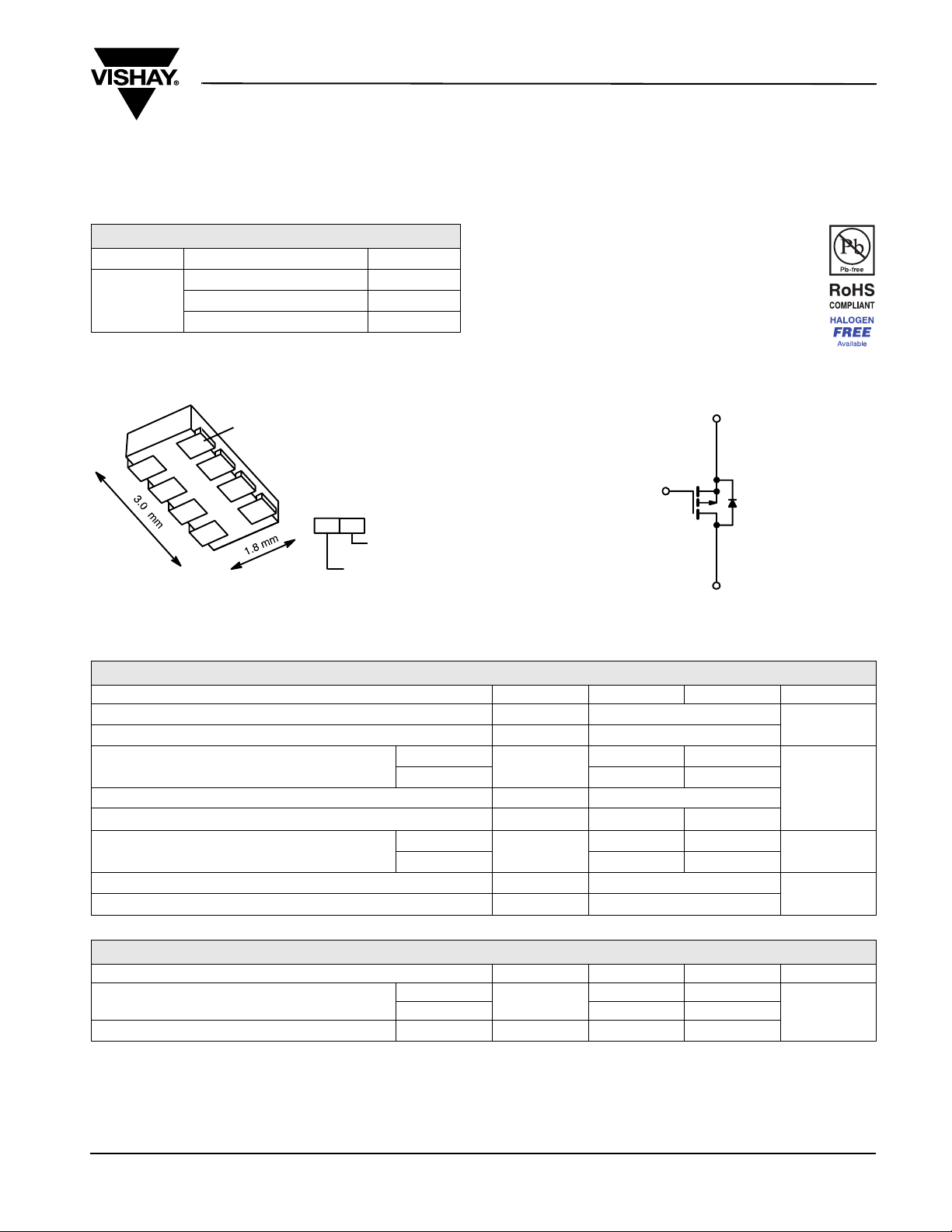
P-Channel 20-V (D-S) MOSFET
T
Si5447DC
Vishay Siliconix
PRODUCT SUMMARY
VDS (V) R
0.076 at V
- 20
0.110 at V
0.160 at V
1206-8 ChipFET
D
D
Ordering Information: Si5447DC-T1-E3 (Lead (Pb)-free)
Si5447DC-T1-GE3 (Lead (Pb)-free and Halogen-free)
D
D
Bottom View
D
D
S
(Ω)I
DS(on)
= - 4.5 V
GS
= - 2.5 V
GS
= - 1.8 V
GS
®
1
G
Marking Code
BG XX
Part #
Code
Lot Traceability
and Date Code
(A)
D
- 4.8
- 4.0
- 3.3
FEATURES
• Halogen-free According to IEC 61249-2-21
Available
• TrenchFET
®
Power MOSFETs: 1.8 V Rated
S
G
D
P-Channel MOSFE
ABSOLUTE MAXIMUM RATINGS TA = 25 °C, unless otherwise noted
Parameter Symbol 5 s Steady State Unit
Drain-Source Voltage
Gate-Source Voltage
Continuous Drain Current (T
= 150 °C)
J
a
Pulsed Drain Current
Continuous Source Current
Maximum Power Dissipation
a
a
Operating Junction and Storage Temperature Range
Soldering Recommendations (Peak Temperature)
b, c
TA = 25 °C
= 85 °C
T
A
TA = 25 °C
= 85 °C
T
A
V
DS
V
GS
I
D
I
DM
I
S
P
D
T
, T
J
stg
- 4.8 - 3.5
- 3.5 - 2.5
- 2.1 - 1.1
- 20
± 8
- 15
2.5 1.3
1.3 0.7
- 55 to 150
260
V
A
W
°C
THERMAL RESISTANCE RATINGS
Parameter Symbol Typical Maximum Unit
Maximum Junction-to-Ambient
a
Maximum Junction-to-Foot (Drain) Steady State
Notes:
a. Surface Mounted on 1" x 1" FR4 board.
t ≤ 5 s
Steady State 83 95
R
thJA
R
thJF
b. See Reliability Manual for profile. The ChipFET is a leadless package. The end of the lead terminal is exposed copper (not plated) as a result
of the singulation process in manufacturing. A solder fillet at the exposed copper tip cannot be guaranteed and is not required to ensure
adequate bottom side solder interconnection.
c. Rework Conditions: manual soldering with a soldering iron is not recommended for leadless components.
Document Number: 71256
S09-0129-Rev. C, 02-Feb-09
43 50
°C/W
14 20
www.vishay.com
1
Si5447DC
Vishay Siliconix
SPECIFICATIONS TJ = 25 °C, unless otherwise noted
Parameter Symbol Test Conditions Min. Typ. Max. Unit
Static
V
Gate Threshold Voltage
Gate-Body Leakage
Zero Gate Voltage Drain Current
On-State Drain Current
a
Drain-Source On-State Resistance
Forward Transconductance
Diode Forward Voltage
Dynamic
b
a
a
Total Gate Charge
Gate-Drain Charge
Tur n -O n De l ay T i m e
Rise Time
Turn-Off Delay Time
Fall Time
Source-Drain Reverse Recovery Time
V
GS(th)
I
GSS
I
DSS
I
D(on)
a
R
DS(on)
g
fs
V
SD
Q
g
Q
gs
Q
gd
t
d(on)
t
r
t
d(off)
t
f
t
rr
V
V
V
DS
I
D
Notes:
a. Pulse test; pulse width ≤ 300 µs, duty cycle ≤ 2 %.
b. Guaranteed by design, not subject to production testing.
Stresses beyond those listed under “Absolute Maximum Ratings” may cause permanent damage to the de vice. These are stress rating s only, and functiona l operation
of the device at these or any other conditions beyond those indicated in the operational sections of the specifications is not implied. Exposure to absolute maximum
rating conditions for extended periods may affect device reliability.
= VGS, ID = - 250 µA
DS
VDS = 0 V, VGS = ± 8 V
V
= - 16 V, V
DS
= - 16 V, V
DS
≤ - 5 V, V
DS
V
= - 4.5 V, ID = - 3.5 A
GS
V
= - 2.5 V, ID = - 2.9 A
GS
V
= - 1.8 V, ID = - 1 A
GS
GS
= 0 V
GS
= 0 V, TJ = 85 °C
= - 4.5 V
GS
VDS = - 10 V, ID = - 3.5 A
IS = - 1.1 A, V
= - 10 V, V
V
= - 10 V, RL = 10 Ω
DD
≅ - 1 A, V
GEN
GS
= 0 V
GS
= - 4.5 V, ID = - 3.5 A
= - 4.5 V, RG = 6 Ω
IF = - 1.1 A, dI/dt = 100 A/µs
- 0.45 V
± 100 nA
- 1
- 5
- 15 A
0.064 0.076
0.091 0.110
0.130 0.160
9S
- 0.8 - 1.2 V
6.5 10
1.4
1.3
14 21
29 45
42 65
35 55
30 60
µA
Ω
nCGate-Source Charge
ns
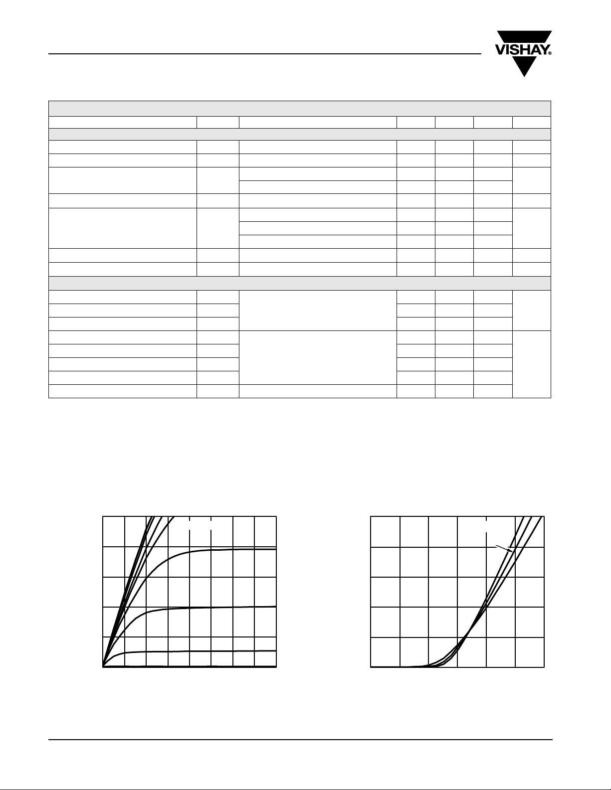
TYPICAL CHARACTERISTICS 25 °C, unless otherwise noted
15
12
9
6
- Drain Current (A)I
D
3
0
0.0 0.5 1.0 1.5 2.0 2.5 3.0 3.5 4.0
www.vishay.com
2
V
DS
VGS=5thru3V
2.5 V
2V
1.5 V
1V
- Drain-to-Source Voltage (V)
Output Characteristics
15
TC= - 55 °C
12
9
6
- Drain Current (A)I
D
3
0
0.0 0.5 1.0 1.5 2.0 2.5 3.0
VGS- Gate-to-Source Voltage (V)
25 °C
Transfer Characteristics
Document Number: 71256
S09-0129-Rev. C, 02-Feb-09
125 °C
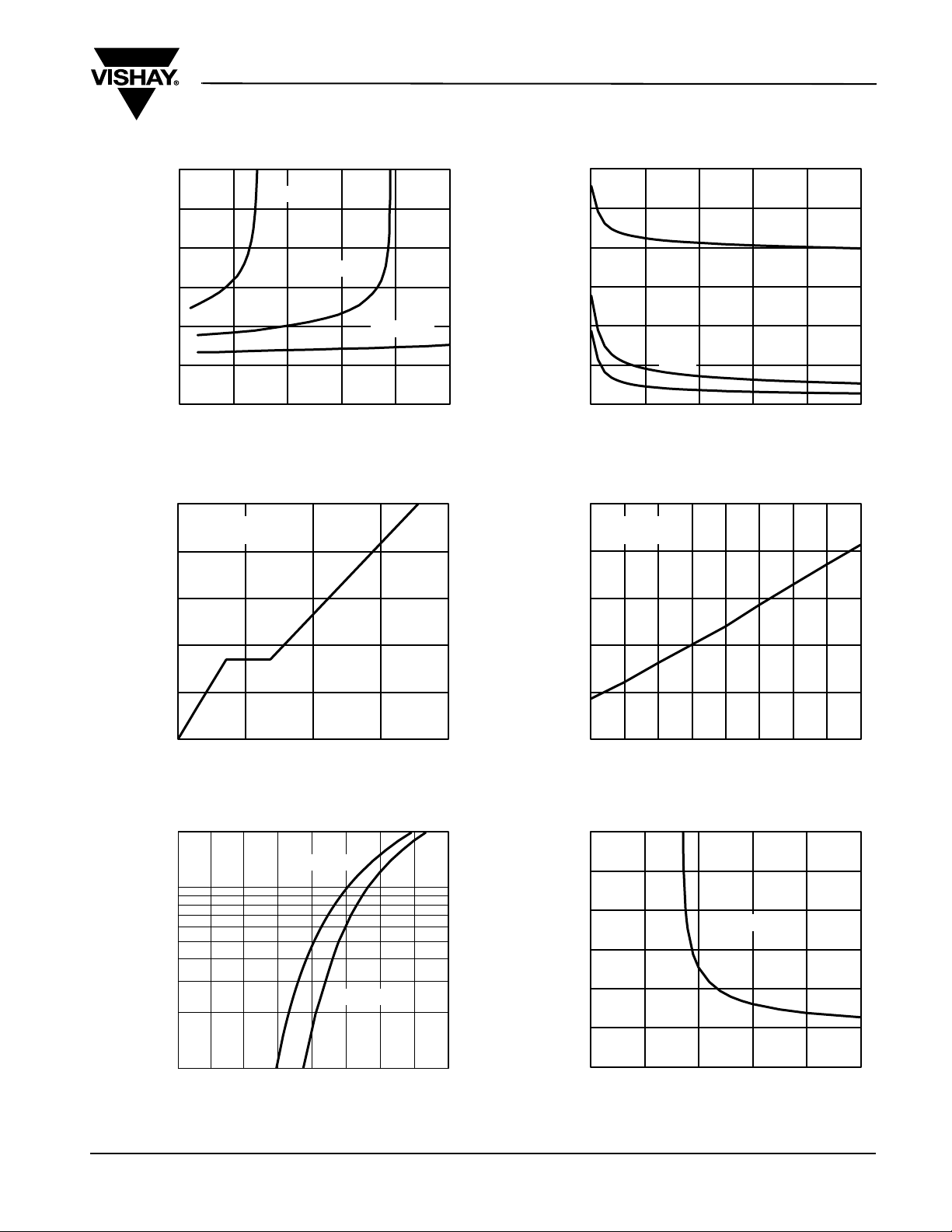
TYPICAL CHARACTERISTICS 25 °C, unless otherwise noted
0.30
0.25
0.20
0.15
- On-Resistance (Ω)R
0.10
DS(on)
0.05
0.00
03691215
On-Resistance vs. Drain Current
VGS= 1.8 V
VGS= 2.5 V
- Drain Current (A)
I
D
VGS=4.5V
C - Capacitance (pF)
Si5447DC
Vishay Siliconix
1200
1000
C
iss
800
600
400
C
200
C
rss
0
0 4 8 121620
oss
- Drain-to-Source Voltage (V)
V
DS
Capacitance
5
VDS=10V
I
=3.5A
D
4
3
2
- Gate-to-Source Voltage (V)
GS
1
V
0
02468
Qg- Total Gate Charge (nC)
Gate Charge
20
TJ= 150 °C
10
- Source Current (A)I
S
TJ=25°C
1.6
VGS=4.5V
I
=3.5A
D
1.4
1.2
- On-ResistanceR
1.0
(Normalized)
DS(on)
0.8
0.6
- 50 - 25 0 25 50 75 100 125 150
- Junction Temperature (°C)
T
J
On-Resistance vs. Junction Temperature
0.30
0.25
0.20
0.15
- On-Resistance (Ω)R
0.10
DS(on)
0.05
ID=3.5A
1
0.0 0.2 0.4 0.6 0.8 1.0 1.2 1.4 1.6
VSD- Source-to-Drain Voltage (V)
Source-Drain Diode Forward Voltage
Document Number: 71256
S09-0129-Rev. C, 02-Feb-09
0.00
012345
VGS- Gate-to-Source Voltage (V)
On-Resistance vs. Gate-to-Source Voltage
www.vishay.com
3

Si5447DC
Vishay Siliconix
TYPICAL CHARACTERISTICS 25 °C, unless otherwise noted
0.4
50
0.3
ID= 250 µA
0.2
0.1
Variance (V)V
GS(th)
0.0
-0.1
-0.2
- 50 - 25 0 25 50 75 100 125 150
TJ- Temperature (°C)
Threshold Voltage
2
1
Duty Cycle = 0.5
0.2
0.1
0.1
Thermal Impedance
Normalized Effective Transient
0.05
0.02
Single Pulse
0.01
-4
10
-3
10
Normalized Thermal Transient Impedance, Junction-to-Ambient
2
40
30
Pow er (W)
20
10
0
0
-2
10
-1
1 100 6001010
Time (s)
Single Pulse Power
Notes:
P
DM
t
1
t
2
t
1. Duty Cycle, D =
2. Per Unit Base = R
3. T
JM-TA=PDMZthJA
4. Surface Mounted
-2
10
-1
1 10 60010
Square Wave Pulse Duration (s)
t
thJA
100
1
2
(t)
=80 °C/W
1
Duty Cycle = 0.5
0.2
0.1
0.1
Thermal Impedance
Normalized Effective Transient
0.05
0.02
Single Pulse
0.01
-4
10
-3
10
-2
10
-1
11010
Square Wave Pulse Duration (s)
Normalized Thermal Transient Impedance, Junction-to-Foot
Vishay Siliconix maintains worldwide manufacturing capability. Products may be manufactured at one of several qualified locations. Reliability data for Silicon
Technology and Package Reliability represent a composite of all qualified locations. For related documents such as package/tape drawings, part marking, and
reliability data, see www.vishay.com/ppg?71256
www.vishay.com
4
.
Document Number: 71256
S09-0129-Rev. C, 02-Feb-09

1206-8 ChipFETR
Package Information
Vishay Siliconix
4
D
6578
4
3421
S b
NOTES:
1. All dimensions are in millimeaters.
2. Mold gate burrs shall not exceed 0.13 mm per side.
3. Leadframe to molded body offset is horizontal and vertical shall not exceed
4. Dimensions exclusive of mold gate burrs.
5. No mold flash allowed on the top and bottom lead surface.
e
0.08 mm.
EE
1
2X 0.10/0.13 R
A
L
5678
4321
c
x
C1
Backside View
DETAIL X
Document Number: 71151
15-Jan-04
MILLIMETERS INCHES
Dim Min Nom Max Min Nom Max
1.00 − 1.10 0.039 − 0.043
A
0.25 0.30 0.35 0.010 0.012 0.014
b
0.1 0.15 0.20 0.004 0.006 0.008
c
c1
D
E
E
e
L
S
ECN: C-03528—Rev. F, 19-Jan-04
DWG: 5547
0 − 0.038 0 − 0.0015
2.95 3.05 3.10 0.116 0.120 0.122
1.825 1.90 1.975 0.072 0.075 0.078
1.55 1.65 1.70 0.061 0.065 0.067
1
0.65 BSC 0.0256 BSC
0.28 − 0.42 0.011 − 0.017
0.55 BSC 0.022 BSC
5_Nom 5_Nom
www.vishay.com
1

AN811
Vishay Siliconix
Single-Channel 1206-8 ChipFETr Power MOSFET Recommended
Pad Pattern and Thermal Performance
INTRODUCTION
New Vishay Siliconix ChipFETs in the leadless 1206-8
package feature the same outline as popular 1206-8 resistors
and capacitors but provide all the performance of true power
semiconductor devices. The 1206-8 ChipFET has the same
footprint as the body of the LITTLE FOOTR TSOP-6, and can
be thought of as a leadless TSOP-6 for purposes of visualizing
board area, but its thermal performance bears comparison
with the much larger SO-8.
This technical note discusses the single-channel ChipFET
1206-8 pin-out, package outline, pad patterns, evaluation
board layout, and thermal performance.
PIN-OUT
Figure 1 shows the pin-out description and Pin 1 identification
for the single-channel 1206-8 ChipFET device. The pin-out is
similar to the TSOP-6 configuration, with two additional drain
pins to enhance power dissipation and thermal performance.
The legs of the device are very short, again helping to reduce
the thermal path to the external heatsink/pcb and allowing a
larger die to be fitted in the device if necessary.
Single 1206-8 ChipFET
1
D
D
D
D
D
D
G
S
26 mil
FIGURE 2. Footprint With Copper Spreading
The pad pattern with copper spreading shown in Figure 2
improves the thermal area of the drain connections (pins
1,2,3,6.7,8) while remaining within the confines of the basic
footprint. The drain copper area is 0.0054 sq. in. or
3.51 sq. mm). This will assist the power dissipation path away
from the device (through the copper leadframe) and into the
board and exterior chassis (if applicable) for the single device.
The addition of a further copper area and/or the addition of vias
to other board layers will enhance the performance still further.
An example of this method is implemented on the
Vishay Siliconix Evaluation Board described in the next
section (Figure 3).
THE VISHAY SILICONIX EVALUATION
BOARD FOR THE SINGLE 1206-8
80 mil
68 mil
28 mil
Bottom View
FIGURE 1.
For package dimensions see the 1206-8 ChipFET package
outline drawing (http://www.vishay.com/doc?71151).
BASIC PAD PATTERNS
The basic pad layout with dimensions is shown in Application
Note 826, Recommended Minimum Pad Patterns With Outline
Drawing Access for Vishay Siliconix MOSFETs,
(http://www.vishay.com/doc?72286). This is sufficient for low
power dissipation MOSFET applications, but power
semiconductor performance requires a greater copper pad
area, particularly for the drain leads.
Document Number: 71126
12-Dec-03
The ChipFET 1206-08 evaluation board measures 0.6 in by
0.5 in. Its copper pad pattern consists of an increased pad area
around the six drain leads on the top-side—approximately
0.0482 sq. in. 31.1 sq. mm—and vias added through to the
underside of the board, again with a maximized copper pad
area of approximately the board-size dimensions. The outer
package outline is for the 8-pin DIP, which will allow test
sockets to be used to assist in testing.
The thermal performance of the 1206-8 on this board has been
measured with the results following on the next page. The
testing included comparison with the minimum recommended
footprint on the evaluation board-size pcb and the industry
standard one-inch square FR4 pcb with copper on both sides
of the board.
www.vishay.com
1

AN811
Vishay Siliconix
Front of Board
ChipFETr
FIGURE 3.
THERMAL PERFORMANCE
Junction-to-Foot Thermal Resistance
(the Package Performance)
Thermal performance for the 1206-8 ChipFET measured as
junction-to-foot thermal resistance is 15_C/W typical, 20_C/W
maximum for the single device. The “foot” is the drain lead of
the device as it connects with the body. This is identical to the
SO-8 package R
shortening the leads to the point where they become only a
small part of the total footprint area.
Junction-to-Ambient Thermal Resistance
(dependent on pcb size)
The typical R
80_C/W steady state, compared with 68_C/W for the SO-8.
Maximum ratings are 95_C/W for the 1206-8 versus 80_C/W
for the SO-8.
performance, a feat made possible by
Q
jf
for the single-channel 1206-8 ChipFET is
Q
ja
Back of Board
vishay.com
The results show that a major reduction can be made in the
thermal resistance by increasing the copper drain area. In this
example, a 45_C/W reduction was achieved without having to
increase the size of the board. If increasing board size is an
option, a further 33_C/W reduction was obtained by
maximizing the copper from the drain on the larger 1” square
pcb.
160
120
80
40
Thermal Resistance (C/W)
Min. Footprint
Single EVB
1” Square PCB
Testing
To aid comparison further, Figure 4 illustrates ChipFET 1206-8
thermal performance on two different board sizes and three
different pad patterns. The results display the thermal
performance out to steady state and produce a graphic
account of how an increased copper pad area for the drain
connections can enhance thermal performance. The
measured steady state values of R
for the single 1206-8
Q
ja
ChipFET are :
1) Minimum recommended pad pattern (see
156_C/W
Figure 2) on the evaluation board size of
0.5 in x 0.6 in.
2) The evaluation board with the pad pattern
111_C/W
described on Figure 3.
3) Industry standard 1” square pcb with
78_C/W
maximum copper both sides.
www.vishay.com
2
0
-5
10
10
-3
-4
10
FIGURE 4. Single 1206−8 ChipFET
-2
10
Time (Secs)
-1
1
1010
100 1000
SUMMARY
The thermal results for the single-channel 1206-8 ChipFET
package display similar power dissipation performance to the
SO-8 with a footprint reduction of 80%. Careful design of the
package has allowed for this performance to be achieved. The
short leads allow the die size to be maximized and thermal
resistance to be reduced within the confines of the TSOP-6
body size.
ASSOCIATED DOCUMENT
1206-8 ChipFET Dual Thermal performance, AN812
(http://www.vishay.com/doc?71127).
Document Number: 71126
12-Dec-03

Application Note 826
Vishay Siliconix
RECOMMENDED MINIMUM PADS FOR 1206-8 ChipFET
0.093
(2.357)
0.080
(2.032)
®
0.036
(0.914)
0.022
(0.559)
Return to Index
Return to Index
0.026
(0.650)
0.016
(0.406)
Recommended Minimum Pads
Dimensions in Inches/(mm)
0.010
(0.244)
APPLICATION NOTE
www.vishay.com Document Number: 72593
2 Revision: 21-Jan-08

Legal Disclaimer Notice
www.vishay.com
Vishay
Disclaimer
ALL PRODUCT, PRODUCT SPECIFICATIONS AND DATA ARE SUBJECT TO CHANGE WITHOUT NOTICE TO IMPROVE
RELIABILITY, FUNCTION OR DESIGN OR OTHERWISE.
Vishay Intertechnology, Inc., its affiliates, agents, and employees, and all persons acting on its or their behalf (collectively,
“Vishay”), disclaim any and all liability for any errors, inaccuracies or incompleteness contained in any datasheet or in any other
disclosure relating to any product.
Vishay makes no warranty, representation or guarantee regarding the suitability of the products for any particular purpose or
the continuing production of any product. To the maximum extent permitted by applicable law, Vishay disclaims (i) any and all
liability arising out of the application or use of any product, (ii) any and all liability, including without limitation special,
consequential or incidental damages, and (iii) any and all implied warranties, including warranties of fitness for particular
purpose, non-infringement and merchantability.
Statements regarding the suitability of products for certain types of applications are based on Vishay’s knowledge of typical
requirements that are often placed on Vishay products in generic applications. Such statements are not binding statements
about the suitability of products for a particular application. It is the customer’s responsibility to validate that a particular
product with the properties described in the product specification is suitable for use in a particular application. Parameters
provided in datasheets and/or specifications may vary in different applications and performance may vary over time. All
operating parameters, including typical parameters, must be validated for each customer application by the customer’s
technical experts. Product specifications do not expand or otherwise modify Vishay’s terms and conditions of purchase,
including but not limited to the warranty expressed therein.
Except as expressly indicated in writing, Vishay products are not designed for use in medical, life-saving, or life-sustaining
applications or for any other application in which the failure of the Vishay product could result in personal injury or death.
Customers using or selling Vishay products not expressly indicated for use in such applications do so at their own risk. Please
contact authorized Vishay personnel to obtain written terms and conditions regarding products designed for such applications.
No license, express or implied, by estoppel or otherwise, to any intellectual property rights is granted by this document or by
any conduct of Vishay. Product names and markings noted herein may be trademarks of their respective owners.
Material Category Policy
Vishay Intertechnology, Inc. hereby certifies that all its products that are identified as RoHS-Compliant fulfill the
definitions and restrictions defined under Directive 2011/65/EU of The European Parliament and of the Council
of June 8, 2011 on the restriction of the use of certain hazardous substances in electrical and electronic equipment
(EEE) - recast, unless otherwise specified as non-compliant.
Please note that some Vishay documentation may still make reference to RoHS Directive 2002/95/EC. We confirm that
all the products identified as being compliant to Directive 2002/95/EC conform to Directive 2011/65/EU.
Vishay Intertechnology, Inc. hereby certifies that all its products that are identified as Halogen-Free follow Halogen-Free
requirements as per JEDEC JS709A standards. Please note that some Vishay documentation may still make reference
to the IEC 61249-2-21 definition. We confirm that all the products identified as being compliant to IEC 61249-2-21
conform to JEDEC JS709A standards.
Revision: 02-Oct-12
1
Document Number: 91000

 Loading...