

查询SI4980DY供应商
PRODUCT SUMMARY
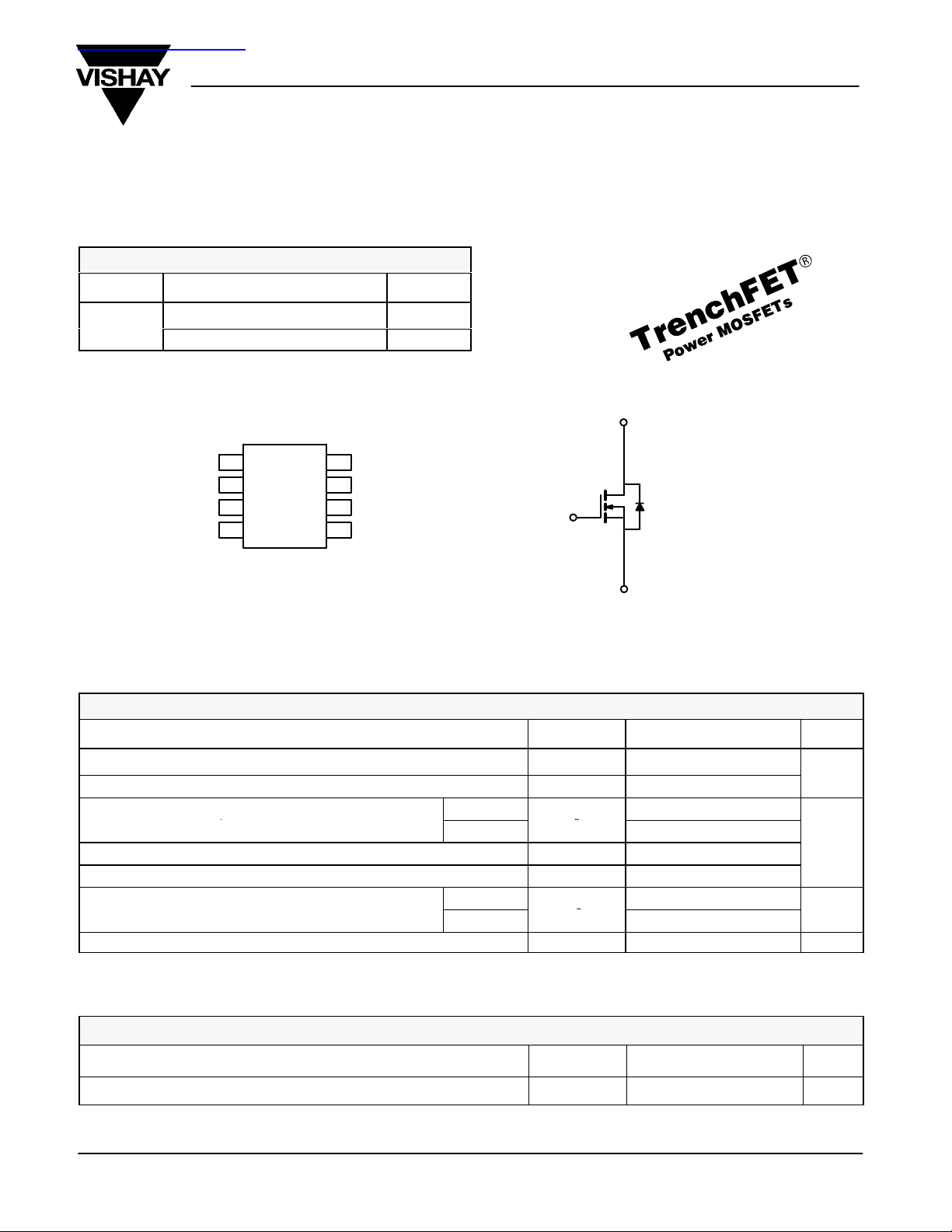
Si4980DY
Vishay Siliconix
Dual N-Channel 80-V (D-S) MOSFET
V
(V) r
DS
80
0.075 @ VGS = 10 V 3.7
0.095 @ VGS = 6.0 V 3.2
(W) I
DS(on)
(A)
D
D
SO-8
S
1
1
G
2
1
S
3
2
G
4
2
Top View
Ordering Information: Si4980DY
Si4980DY-T1 (with Tape and Reel)
D
1
8
D
7
1
D
6
2
D
5
2
G
S
N-Channel MOSFET
ABSOLUTE MAXIMUM RATINGS (TA = 25_C UNLESS OTHERWISE NOTED)
Parameter Symbol Limit Unit
Drain-Source Voltage V
Gate-Source Voltage V
a
Continuous Drain Current (TJ = 150_C)
Pulsed Drain Current I
Continuous Source Current (Diode Conduction)
Maximum Power Dissipation
Operating Junction and Storage Temperature Range TJ, T
_
a
a
TA = 25_C
TA = 70_C
TA = 25_C
TA = 70_C
THERMAL RESISTANCE RATINGS
Parameter Symbol Limit Unit
Maximum Junction-to-Ambient
Notes
a. Surface Mounted on FR4 Board, t v 10 sec.
Document Number: 70646
S-03950—Rev. D, 26-May-03
a
DS
GS
I
D
DM
I
S
P
D
stg
R
thJA
80
"20
3.7
2.9
30
1.7
2.0
1.3
-55 to 150 _C
62.5 _C/W
www.vishay.com
V
A
W
2-1
Si4980DY
VDD = 40 V, RL = 40 W
Vishay Siliconix
SPECIFICATIONS (TJ = 25_C UNLESS OTHERWISE NOTED)
Parameter Symbol Test Condition Min Typ Max Unit
Static
Gate Threshold Voltage V
Gate-Body Leakage I
Zero Gate Voltage Drain Current I
On-State Drain Curren
Drain-Source On-State Resistance
Forward Transconductance
Diode Forward Voltage
Dynamic
b
a
a
a
a
GS(th)
GSS
DSS
I
D(on)
r
DS(on)
g
V
fs
SD
Total Gate Charge Q
Gate-Source Charge Q
Gate-Drain Charge Q
gs
gd
Gate Resistance R
Turn-On Delay Time t
Rise Time t
Turn-Off Delay Time t
Fall Time t
Source-Drain Reverse Recovery Time t
Notes
a. Pulse test; pulse width v
b. For design aid only; not subject to production testing.
300 ms, duty cycle v 2%.
d(on)
r
d(off)
f
rr
VDS = VGS, I
VDS = 0 V, VGS = "20 V
VDS = 80 V, VGS = 0 V
VDS = 80 V, VGS = 0 V, TJ = 55_C
= 250 mA 2 V
D
"100 nA
1
20
mA
VDS = 5 V, VGS = 10 V 20 A
VGS = 10 V, ID = 3.7 A 0.062 0.075
VGS = 6.0 V, ID = 3.2 A 0.071 0.095
W
VDS = 15 V, ID = 3.7 A 12 S
IS = 1.7 A, VGS = 0 V 1.2 V
g
V
= 40 V, VGS = 10 V, ID = 3.7 A 4 nC
DS
15 30
3.2
g
1 5.1 W
10 20
VDD = 40 V, RL = 40 W
ID ^ 1 A, V
GEN
= 10 V, RG = 6 W
10 20
30 60
ns
10 20
IF = 1.7 A, di/dt = 100 A/ms 75 110
www.vishay.com
2-2
Document Number: 70646
S-03950—Rev. D, 26-May-03

TYPICAL CHARACTERISTICS (25_C UNLESS NOTED)
Si4980DY
Vishay Siliconix
30
24
VGS = 10 thru 6 V
18
12
- Drain Current (A)I
D
6
0
012345
VDS - Drain-to-Source Voltage (V)
On-Resistance vs. Drain Current
0.20
0.16
W )
Output Characteristics Transfer Characteristics
0.12
0.08
- On-Resistance (r
DS(on)
0.04
VGS = 6 V
VGS = 10 V
5 V
4 V
30
24
18
12
- Drain Current (A)I
D
6
0
01234567
V
GS
TC = 125_C
25_C
-55_C
- Gate-to-Source Voltage (V)
Capacitance
1200
900
600
C - Capacitance (pF)
300
C
C
oss
rss
C
iss
0.00
0 6 12 18 24 30
10
VDS = 40 V
8
I
= 3.7 A
D
6
4
- Gate-to-Source Voltage (V)
2
GS
V
0
0 3 6 9 12 15
Document Number: 70646
S-03950—Rev. D, 26-May-03
ID - Drain Current (A)
Gate Charge
Qg - Total Gate Charge (nC)
2.0
1.6
W )
1.2
0.8
(Normalized)
- On-Resistance (r
0.4
DS(on)
0.0
0
0 102030405060
V
- Drain-to-Source Voltage (V)
DS
On-Resistance vs. Junction Temperature
VGS = 10 V
I
= 3.7 A
D
-50 -25 0 25 50 75 100 125 150
T
- Junction Temperature (_C)
J
www.vishay.com
2-3

Si4980DY
Vishay Siliconix
TYPICAL CHARACTERISTICS (25_C UNLESS NOTED)
Source-Drain Diode Forward Voltage On-Resistance vs. Gate-to-Source Voltage
20
10
TJ = 150_C
- Source Current (A)I
S
1
0 0.2 0.4 0.6 0.8 1.0 1.2
VSD - Source-to-Drain Voltage (V) VGS - Gate-to-Source Voltage (V)
Threshold Voltage Single Pulse Power
1.0
0.5
ID = 250 mA
0.0
Variance (V)V
GS(th)
-0.5
TJ = 25_C
0.20
0.15
W )
ID = 3.7 A
0.10
- On-Resistance (r
0.05
DS(on)
0.00
0246810
50
40
30
20
Power (W)
10
-1.0
-50 -25 0 25 50 75 100 125 150
2
1
0.1
Thermal Impedance
Normalized Effective Transient
0.01
www.vishay.com
2-4
Duty Cycle = 0.5
0.2
0.1
0.05
0.02
-4
10
0
0.01 0.10 1.00 10.00
TJ - Temperature (_C) Time (sec)
Normalized Thermal Transient Impedance, Junction-to-Ambient
Notes:
P
DM
t
1
t
2
thJA
Single Pulse
-3
10
-2
10
-1
10
Square Wave Pulse Duration (sec)
1. Duty Cycle, D =
2. Per Unit Base = R
3. TJM - TA = PDMZ
4. Surface Mounted
11030
t
1
t
2
= 62.5_C/W
thJA
(t)
Document Number: 70646
S-03950—Rev. D, 26-May-03
 Loading...