

Si4858DY
30
PRODUCT SUMMARY
V
(V)
DS
r
DS(on)
0.00525 @ VGS = 10 V 20
0.007 @ VGS = 4.5 V 17
SD
1
SD
2
SD
3
GD
4
New Product
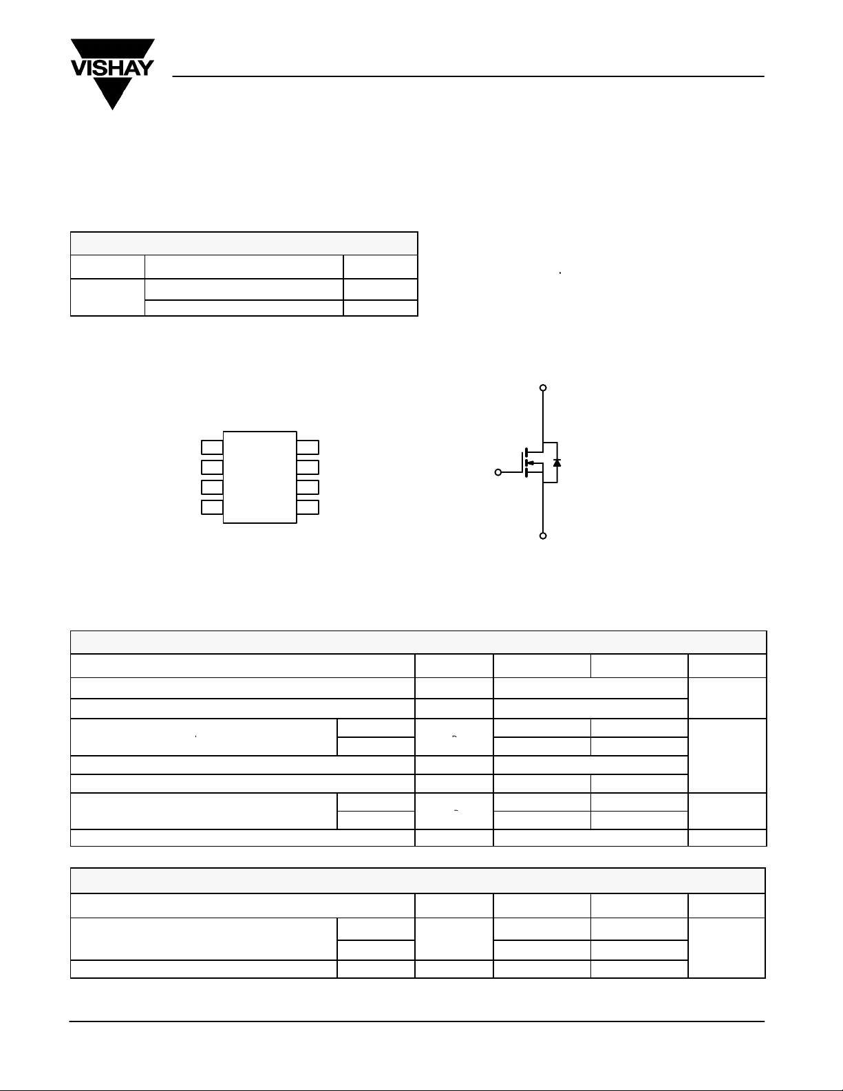
N-Channel 30-V (D-S) MOSFET
FEATURES
D TrenchFETr Power MOSFET
D Optimized for “Low Side” Synchronous
(W)
SO-8
I
(A)
D
8
7
6
5
Rectifier Operation
D 100% R
APPLICATIONS
D DC/DC Converters
D Synchronous Rectifiers
D
G
Tested
G
Vishay Siliconix
Top View
S
N-Channel MOSFET
ABSOLUTE MAXIMUM RATINGS (TA = 25_C UNLESS OTHERWISE NOTED)
Parameter Symbol 10 secs Steady State Unit
Drain-Source Voltage V
Gate-Source Voltage V
a
Continuous Drain Current (TJ = 150_C)
Pulsed Drain Current (10 ms Pulse Width)
Continuous Source Current (Diode Conduction)
Maximum Power Dissipation
Operating Junction and Storage Temperature Range TJ, T
_
a
a
TA = 25_C
TA = 70_C
TA = 25_C
TA = 70_C
I
P
I
DM
I
DS
GS
D
20 13
15 10
S
D
stg
2.9 1.3
3.5 1.6
2.2 1
30
"20
60
-55 to 150
THERMAL RESISTANCE RATINGS
Parameter Symbol Typical Maximum Unit
Maximum Junction-to-Ambient
Maximum Junction-to-Foot (Drain) Steady State R
Notes
a. Surface Mounted on 1” x 1” FR4 Board.
a
t v 10 sec
Steady State
R
thJA
thJF
29 35
67 80
13 16
V
A
W
_C
_C/W
Document Number: 70690
S-03662—Rev. B, 14-Apr-03
www.vishay.com
1
Si4858DY
Drain-Source On-State Resistance
a
W
VDD = 15 V, RL = 15 W
Vishay Siliconix
New Product
SPECIFICATIONS (TJ = 25_C UNLESS OTHERWISE NOTED)
Parameter Symbol Test Condition Min Typ Max Unit
Static
Gate Threshold Voltage V
Gate-Body Leakage I
Zero Gate Voltage Drain Current I
On-State Drain Current
-
Forward Transconductance
Diode Forward Voltage
Dynamic
b
a
-
a
a
a
Total Gate Charge Q
Gate-Source Charge Q
Gate-Drain Charge Q
Gate Resistance R
Turn-On Delay Time t
Rise Time t
Turn-Off Delay Time t
Fall Time t
Source-Drain Reverse Recovery Time t
GS(th)
GSS
DSS
I
D(on)
r
DS(on)
g
V
d(on)
d(off)
fs
SD
g
gs
gd
G
r
f
rr
Notes
a. Pulse test; pulse width v
b. Guaranteed by design, not subject to production testing.
300 ms, duty cycle v 2%.
VDS = VGS, I
VDS = 0 V, VGS = "20 V "100
VDS = 24 V, VGS = 0 V 1
VDS = 24 V, VGS = 0 V, TJ = 55_C
VDS w 5 V , V
V
GS
VGS = 4.5 V, ID = 19 A 0.0055 0.007
VDS = 15 V, ID = 20 A 90 S
IS = 2.9 A, VGS = 0 V 0.75 1.1 V
V
= 15 V, VGS = 4.5 V, ID = 20 A
DS
VDD = 15 V, RL = 15 W
ID ^ 1 A, V
IF = 2.9 A, di/dt = 100 A/ms
= 10 V, I
= 10 V, RG = 6 W
GEN
= 250 mA
D
= 10 V
GS
= 20 A
D
1.0 V
5
30 A
0.0040 0.00525
30.5 40
13.5
9.5
0.5 1.4 2.4
21 35
10 20
83 130
27 45
50 80
nA
mA
nC
W
ns
TYPICAL CHARACTERISTICS (25_C UNLESS NOTED)
60
50
40
30
20
- Drain Current (A)I
D
10
0
012345
www.vishay.com
2
Output Characteristics Transfer Characteristics
VGS = 10 thru 4 V
VDS - Drain-to-Source Voltage (V)
3 V
60
50
40
30
20
- Drain Current (A)I
D
10
TC = 125_C
25_C
0
0.0 0.5 1.0 1.5 2.0 2.5 3.0 3.5 4.0
VGS - Gate-to-Source Voltage (V)
Document Number: 70690
S-03662—Rev. B, 14-Apr-03
-55_C
Si4858DY
New Product
TYPICAL CHARACTERISTICS (25_C UNLESS NOTED)
0.010
0.008
W )
0.006
0.004
- On-Resistance (r
DS(on)
0.002
0.000
- Gate-to-Source Voltage (V)
GS
V
10
8
6
4
2
On-Resistance vs. Drain Current
VGS = 4.5 V
VGS = 10 V
0 1020304050
ID - Drain Current (A)
Gate Charge
VDS = 15 V
= 20 A
I
D
W)
- On-Resistance (r
6500
5200
3900
2600
C - Capacitance (pF)
1300
0
0 6 12 18 24 30
1.8
1.6
1.4
1.2
(Normalized)
1.0
DS(on)
0.8
Vishay Siliconix
Capacitance
C
iss
C
C
rss
V
DS
On-Resistance vs. Junction Temperature
VGS = 10 V
= 20 A
I
D
oss
- Drain-to-Source Voltage (V)
0
0 1530456075
Source-Drain Diode Forward Voltage On-Resistance vs. Gate-to-Source Voltage
60
10
- Source Current (A)I
S
1
0.00 0.2 0.4 0.6 0.8
VSD - Source-to-Drain Voltage (V) VGS - Gate-to-Source Voltage (V)
Document Number: 70690
S-03662—Rev. B, 14-Apr-03
Qg - Total Gate Charge (nC)
TJ = 150_C
TJ = 25_C
1.0 1.2
W )
- On-Resistance (r
DS(on)
0.6
-50 -25 0 25 50 75 100 125 150
T
- Junction Temperature (_C)
J
0.020
0.016
0.012
0.008
0.004
0.000
0246810
ID = 20 A
www.vishay.com
3
Si4858DY
Vishay Siliconix
New Product
TYPICAL CHARACTERISTICS (25_C UNLESS NOTED)
0.6
0.4
0.2
-0.0
Variance (V)V
-0.2
GS(th)
-0.4
-0.6
-0.8
-50 -25 0 25 50 75 100 125 150
2
Threshold Voltage
ID = 250 mA
TJ - Temperature (_C)
Normalized Thermal Transient Impedance, Junction-to-Ambient
60
50
40
30
Power (W)
20
10
0
10
Single Pulse Power
-2
-1
1 100 6001010
Time (sec)
1
0.1
Thermal Impedance
Normalized Effective Transient
0.01
10
2
1
0.1
Thermal Impedance
Normalized Effective Transient
Duty Cycle = 0.5
0.2
0.1
0.05
0.02
-4
Duty Cycle = 0.5
0.2
0.1
0.05
0.02
10
-3
Single Pulse
-2
10
-1
1 10 60010
Square Wave Pulse Duration (sec)
Normalized Thermal Transient Impedance, Junction-to-Foot
Notes:
P
DM
t
1
t
- TA = PDMZ
JM
2
1. Duty Cycle, D =
2. Per Unit Base = R
3. T
4. Surface Mounted
thJA
thJA
100
t
1
t
2
= 67_C/W
(t)
0.01
www.vishay.com
4
Single Pulse
-4
10
-3
10
-2
10
-1
11010
Square Wave Pulse Duration (sec)
Document Number: 70690
S-03662—Rev. B, 14-Apr-03
 Loading...