

Si4852DY
)
Continuous Drain Current (TJ = 150 C)
C/W
Vishay Siliconix
N-Channel 30-V (D-S) MOSFET with Schottky Diode
PRODUCT SUMMARY
V
(V) r
DS
30
0.0120 @ VGS = 10 V 11
0.0175 @ VGS = 4.5 V 9.5
(W) I
DS(on)
(A)
D
FEATURES
D LITTLE FOOTr Plus
D 100% R
Tested
g
SCHOTTKY PRODUCT SUMMARY
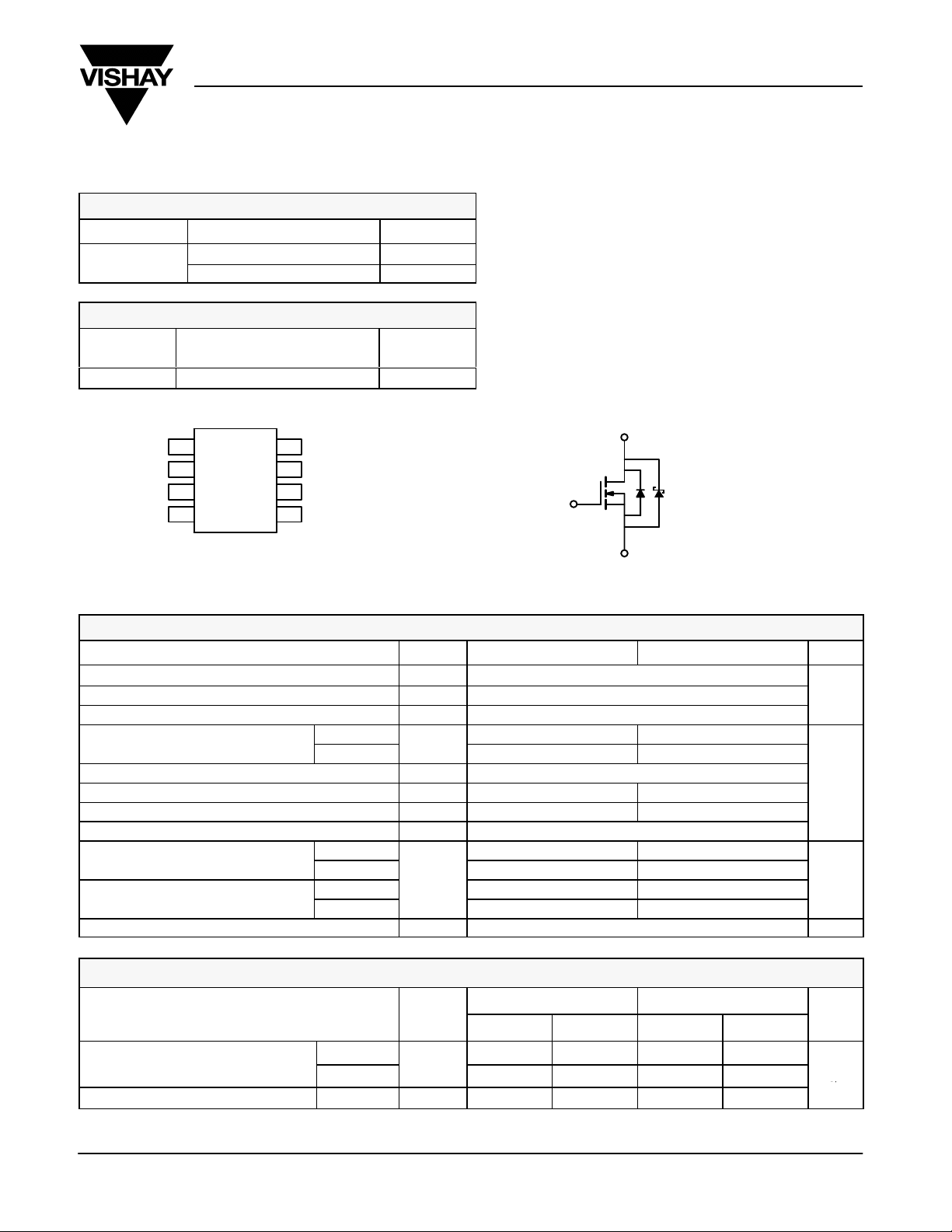
SO-8
Top View
VSD (v)
8
7
6
5
I
(A)
F
D
D
D
G
S
N-Channel MOSFET
Schottky Diode
V
(V)
DS
30 0.53 V @ 3 A 4
SD
S
SD
G
Ordering Information: Si4852DY
Diode Forward Voltage
1
2
3
4
Si4852DY-T1 (with Tape and Reel)
ABSOLUTE MAXIMUM RATINGS (TA = 25_C UNLESS OTHERWISE NOTED)
Parameter Symbol 10 secs Steady State Unit
Drain-Source Voltage (MOSFET) V
Reverse Voltage (Schottky) V
Gate-Source Voltage V
Continuous Drain Current (TJ = 150_C
(MOSFET)
Pulsed Drain Current (MOSFET) I
Continuous Source Current (MOSFET Diode Conduction)
Average Foward Current (Schottky) I
Pulsed Foward Current (Schottky) I
Maximum Power Dissipation (MOSFET)
Maximum Power Dissipation (Schottky)
Operating Junction and Storage Temperature Range TJ, T
a
a
a
TA = 25_C
TA = 70_C
a
TA = 25_C 2.5 1.47
TA = 70_C
TA = 25_C
TA = 70_C 1.45 0.88
P
I
DM
I
FM
DS
DA
GS
D
S
F
D
stg
11 8.7
9.0 7.0
2.3 1.3
4.0 2.5
1.6 0.94
2.27 1.38
30
30
"20
50
50
-55 to 150 _C
V
A
W
THERMAL RESISTANCE RATINGS
Maximum Junction-to-Ambient
Maximum Junction-to-Foot (Drain) Steady-State R
Notes
a. Surface Mounted on 1” x 1” FR4 Board.
Document Number: 71307
S-31726—Rev. D, 18-Aug-03
Parameter Symbol
a
t v 10 sec
Steady-State
MOSFET Schottky
Typ Max Typ Max
R
thJA
thJF
40 50 45 55
72 85 75 90
18 22 20 25
Unit
_C/W
www.vishay.com
1
Si4852DY
g
DSS
b
b
DS
,
GS
,
D
VDD = 15 V, RL = 15 W
g
rm
Vishay Siliconix
MOSFET SPECIFICATIONS (TJ = 25_C UNLESS OTHERWISE NOTED).
Parameter Symbol Test Condition Min TypaMax Unit
Static
Gate Threshold Voltage V
Gate-Body Leakage I
Zero Gate Voltage Drain Current I
On-State Drain Current
b
Drain-Source On-State Resistance
Forward Transconductance
b
Schottky Diode Forward Voltage
Dynamic
a
Total Gate Charge Q
Gate-Source Charge Q
Gate-Drain Charge Q
Gate Resistance R
Turn-On Delay Time t
Rise Time t
Turn-Off Delay Time t
Fall Time t
Source-Drain Reverse Recovery Time t
Notes
a. Guaranteed by design, not subject to production testing.
b. Pulse test; pulse width v
300 ms, duty cycle v 2%.
GS(th)
GSS
DSS
I
D(on)
r
DS(on)
g
V
d(on)
d(off)
fs
SD
g
gs
gd
g
r
f
rr
VDS = VGS, I
VDS = 0 V, V
= 250 mA 1 V
D
= "20 V "100 nA
GS
VDS = 24 V, VGS = 0 V 0.007 0.100
VDS = 24 V, VGS = 0 V, TJ = 100_C 1.5 10
VDS = 24 V, VGS = 0 V, TJ = 125_C 6.5 20
V
5 V, VGS = 10 V 20 A
w
DS
VGS = 10 V, ID = 11 A 0.0100 0.0120
VGS = 4.5 V, ID = 9.5 A 0.0145 0.0175
VDS = 15 V, ID = 11 A 28 S
IS = 3.0 A, VGS = 0 V 0.485 0.53
IS = 3.0 A, VGS = 0 V, TJ = 125_C 0.416 0.47
V
= 15 V, VGS = 5 V, ID = 11 A
DS
VDD = 15 V, RL = 15 W
ID ^ 1 A, V
= 10 V, RG = 6 W
GEN
IF = 3.o A, di/dt = 100 A/ms 40 70
24 35
9
7.5
0.5 2.6 W
17 30
10 20
60 100
18 30
mA
W
V
nC
ns
SCHOTTKY SPECIFICATIONS (TJ = 25_C UNLESS OTHERWISE NOTED)
Parameter Symbol Test Condition Min Typ Max Unit
Forward Voltage Drop V
Maximum Reverse Leakage Current I
Junction Capacitance C
www.vishay.com
2
F
rm
T
IF = 3.0 A 0.485 0.53
IF = 3.0 A, TJ = 125_C 0.416 0.47
Vr = 24 V 0.007 0.100
Vr = 24 V, TJ = 100_C 1.5 10
Vr = -24 V, TJ = 125_C 6.4 20
Vr = 10 V
V
mA
115 pF
Document Number: 71307
S-31726—Rev. D, 18-Aug-03

TYPICAL CHARACTERISTICS (25_C UNLESS NOTED)
Si4852DY
Vishay Siliconix
- Drain Current (A)I
D
W )
- On-Resistance (r
DS(on)
40
Output Characteristics Transfer Characteristics
VGS = 10 thru 4 V
32
24
16
8
2 V
0
0246810
VDS - Drain-to-Source Voltage (V)
0.020
0.016
0.012
0.008
0.004
On-Resistance vs. Drain Current
VGS = 4.5 V
3 V
VGS = 10 V
50
40
30
20
- Drain Current (A)I
D
10
0
0.0 0.5 1.0 1.5 2.0 2.5 3.0 3.5 4.0 4.5
4200
3500
2800
2100
1400
C - Capacitance (pF)
700
TC = 125_C
25_C
VGS - Gate-to-Source Voltage (V)
Capacitance
C
iss
C
oss
C
-55_C
rss
0.000
0 8 16 24 32 40
10
VDS = 15 V
I
= 9.8 A
D
8
6
4
- Gate-to-Source Voltage (V)
GS
2
V
0
0 9 18 27 36 45
Document Number: 71307
S-31726—Rev. D, 18-Aug-03
ID - Drain Current (A)
Gate Charge
Qg - Total Gate Charge (nC)
W)
(Normalized)
- On-Resistance (r
DS(on)
0
0 6 12 18 24 30
VDS - Drain-to-Source Voltage (V)
On-Resistance vs. Junction Temperature
1.8
1.6
1.4
1.2
1.0
0.8
0.6
VGS = 10 V
I
= 9.8 A
D
-50 - 25 0 25 50 75 100 125 150
T
- Junction Temperature (_C)
J
www.vishay.com
3

Si4852DY
Vishay Siliconix
TYPICAL CHARACTERISTICS (25_C UNLESS NOTED)
Source-Drain Diode Forward Voltage
100
TJ = 150_C
10
TJ = 25_C
- Source Current (A)I
1
S
0.1
0.0 0.2 0.4 0.6 0.8 1.0 1.2 1.4
VSD - Source-to-Drain Voltage (V)
Reverse Current (Schottky)
30
10
1
0.1
0.01
- Reverse Curent (mA)I
R
0.001
30 V
10 V
20 V
On-Resistance vs. Gate-to-Source Voltage
0.05
0.04
W )
0.03
0.02
- On-Resistance (
DS(on)
r
0.01
0.00
0246810
100
80
60
Power (W)
40
20
ID = 9.8 A
VGS - Gate-to-Source Voltage (V)
Single Pulse Power, Junction-to-Ambient
0.0001
0 255075100
2
1
0.1
Thermal Impedance
Normalized Effective Transient
0.01
www.vishay.com
4
Duty Cycle = 0.5
0.2
0.1
0.05
0.02
Single Pulse
-4
10
TJ - Temperature (_C)
Normalized Thermal Transient Impedance, Junction-to-Ambient
-3
10
-2
10
125 150
-1
10
Square Wave Pulse Duration (sec)
0
0.001
0.01
1
Time (sec)
Notes:
P
DM
t
1
t
2
t
thJA
100
thJA
1
t
2
= 72_C/W
(t)
1. Duty Cycle, D =
2. Per Unit Base = R
3. TJM - TA = PDMZ
4. Surface Mounted
1 10 600
Document Number: 71307
S-31726—Rev. D, 18-Aug-03
100.1

TYPICAL CHARACTERISTICS (25_C UNLESS NOTED)
Si4852DY
Vishay Siliconix
2
1
0.1
Thermal Impedance
Normalized Effective Transient
0.01
10
Duty Cycle = 0.5
0.2
0.1
0.05
0.02
Single Pulse
-4
Normalized Thermal Transient Impedance, Junction-to-Foot
-3
10
-2
10
Square Wave Pulse Duration (sec)
-1
11010
Document Number: 71307
S-31726—Rev. D, 18-Aug-03
www.vishay.com
5

Legal Disclaimer Notice
Vishay
Notice
Specifications of the products displayed herein are subject to change without notice. Vishay Intertechnology, Inc.,
or anyone on its behalf, assumes no responsibility or liability for any errors or inaccuracies.
Information contained herein is intended to provide a product description only. No license, express or implied, by
estoppel or otherwise, to any intellectual property rights is granted by this document. Except as provided in Vishay's
terms and conditions of sale for such products, Vishay assumes no liability whatsoever, and disclaims any express
or implied warranty, relating to sale and/or use of Vishay products including liability or warranties relating to fitness
for a particular purpose, merchantability, or infringement of any patent, copyright, or other intellectual property right.
The products shown herein are not designed for use in medical, life-saving, or life-sustaining applications.
Customers using or selling these products for use in such applications do so at their own risk and agree to fully
indemnify Vishay for any damages resulting from such improper use or sale.
Document Number: 91000 www.vishay.com
Revision: 08-Apr-05 1
 Loading...