

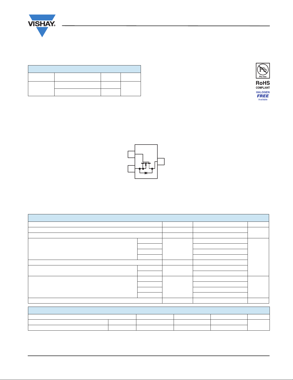
Vishay Si2316BDS Schematic [ru]
N-Channel 30-V (D-S) MOSFET
Si2316BDS
Vishay Siliconix
PRODUCT SUMMARY
VDS (V) R
0.050 at V
30
0.080 at V
(Ω)
DS(on)
= 10 V 4.5
GS
= 4.5 V 3.4
GS
FEATURES
a
(A)
I
D
Qg (Typ)
3.16 nC
• Halogen-free According to IEC 61249-2-21
Definition
• TrenchFET
®
Power MOSFET
• PWM Optimized
• 100 % R
tested
g
• Compliant to RoHS Directive 2002/95/EC
APPLICATIONS
• Battery Switch
• DC/DC Converter
TO-236
(SOT-23)
G
1
D
3
S
2
Top View
Si2316DS (M6)*
*Marking Code
Ordering Information: Si2316BDS-T1-E3 (Lead (Pb)-free)
Si2316BDS-T1-GE3 (Lead (Pb)-free and Halogen-free)
ABSOLUTE MAXIMUM RATINGS TA = 25 °C, unless otherwise noted
Parameter Symbol Limit
Drain-Source Voltage V
Gate-Source Voltage V
T
= 25 °C
C
T
= 70 °C 3.6
Continuous Drain Current (T
= 150 °C)
J
C
= 25 °C
T
A
TA = 70 °C
Pulsed Drain Current I
= 25 °C
T
Continuous Source-Drain Diode Current
Maximum Power Dissipation
C
= 25 °C
T
A
= 25 °C
T
C
T
= 70 °C 1.06
C
= 25 °C
T
A
P
TA = 70 °C
Operating Junction and Storage Temperature Range TJ, T
DS
GS
I
D
DM
I
S
D
stg
30
± 20
4.5
b, c
3.9
b, c
3.13
20
1.39
b, c
1.04
1.66
b, c
1.25
b, c
0.8
- 55 to 150
Unit
V
A
W
°C
THERMAL RESISTANCE RATINGS
Parameter Symbol Typical Maximum Unit
Maximum Junction-to-Ambient
Maximum Junction-to-Foot (Drain) Steady State R
Notes:
a. Based on T
b. Surface mounted on 1" x 1" FR4 moard.
= 25 °C.
C
c. t = 5 s.
d. Maximum under Steady State conditions is 130 °C/W.
b, d
≤ 5 s R
thJA
thJF
80 100
60 75
°C/W
Document Number: 70445
S09-1503-Rev. B, 10-Aug-09
www.vishay.com
1
Si2316BDS
Vishay Siliconix
MOSFET SPECIFICATIONS TJ = 25 °C, unless otherwise noted
Parameter Symbol Test Conditions Min. Typ. Max. Unit
Static
V
Drain-Source Breakdown Voltage V
V
Temperature Coefficient ΔVDS/T
DS
V
Temperature Coefficient
GS(th)
Gate-Source Threshold Voltage V
Gate-Source Leakage I
Zero Gate Voltage Drain Current I
On-State Drain Current
Drain-Source On-State Resistance
Forward Transconductance
Dynamic
b
a
a
a
Input Capacitance C
Output Capacitance C
Reverse Transfer Capacitance C
Total Gate Charge Q
Gate-Source Charge Q
Gate-Drain Charge Q
Gate Resistance R
Tur n - O n D e l ay Time t
Rise Time t
Turn-Off Delay Time t
Fall Ti me t
Tur n - O n D e l ay Time t
Rise Time t
Turn-Off Delay Time t
Fall Ti me t
DS
Δ
J
V
GS(th)/TJ
GS(th)
GSS
DSS
I
V
D(on)
R
DS(on)
g
fs
iss
65
oss
37
rss
g
gs
1.1
gd
f = 1 MHz 2.6 3.9 Ω
g
d(on)
r
12 18
d(off)
f
d(on)
r
11 17
d(off)
f
Drain-Source Body Diode Characteristics
Continuous Source-Drain Diode Current I
Pulse Diode Forward Current
a
Body Diode Voltage V
Body Diode Reverse Recovery Time t
Body Diode Reverse Recovery Charge Q
Reverse Recovery Fall Time t
Reverse Recovery Rise Time t
Notes:
a. Pulse test; pulse width ≤ 300 µs, duty cycle ≤ 2 %.
b. Guaranteed by design, not subject to production testing.
S
I
SM
SD
rr
rr
a
b
V
DS
V
V
DS
V
DS
I
≅ 3.13 A, V
D
I
= 2.4 A, V
D
IF = 2.0 A, dI/dt = 100 A/µs, TJ = 25 °C
= 0 V, ID = 250 µA 30 V
DS
ID = 250 µA
V
= VGS, ID = 250 µA 1 3 V
DS
23.92
5.2
VDS = 0 V, VGS = ± 20 V ± 100 nA
V
= 30 V, V
DS
= 30 V, V
GS
≥ 5 V, V
DS
V
= 10 V, ID = 3.9 A 0.041 0.050
GS
= 4.5 V, ID = 3.3 A 0.064 0.080
V
GS
= 0 V 1
GS
= 0 V, TJ = 55 °C 10
= 10 V 20 A
GS
VDS = 15V, ID = 3.9 A 6 S
350
= 15 V, V
DS
= 15 V, V
= 0 V, f = 1 MHz
GS
= 10 V, ID = 3.9 A 6.35 9.6
GS
3.16 4.8
= 15 V, V
= 4.5 V, ID = 3.9 A
GS
1.56
4.5 6.75
V
= 15 V, RL = 4.8 Ω
DD
= 10 V, RG = 1 Ω
GEN
11 16.5
710.5
20 30
V
= 15 V, RL = 6.25 Ω
DD
= 4.5 V, Rg = 1 Ω
GEN
65 98
23 35
TC = 25 °C 1.39
20
IS = 2.0 A 0.8 1.2 V
10 15 ns
46nC
6.6
3.5
mV/°C
µA
Ω
pF
nC
ns
ns
A
ns
Stresses beyond those listed under “Absolute Maximum Ratings” may cause permanent damage to the device. These are stress ratings only, and functional operation
of the device at these or any other conditions beyond those indicated in the operational sections of the specifications is not implied. Exposure to absolute maximum
rating conditions for extended periods may affect device reliability.
www.vishay.com
2
Document Number: 70445
S09-1503-Rev. B, 10-Aug-09
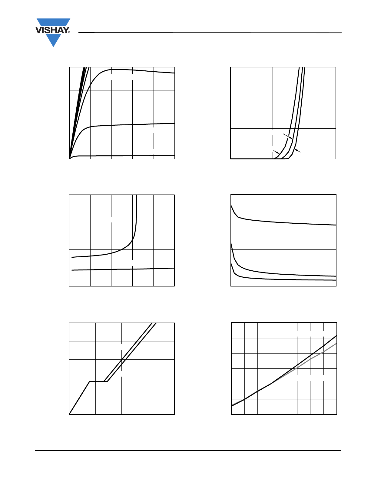
TYPICAL CHARACTERISTICS 25 °C, unless otherwise noted
Si2316BDS
Vishay Siliconix
20
VGS = 10 V thru 5 V
15
10
- Drain Current (A)I
D
5
0
012345
- Drain-to-Source Voltage (V)
V
DS
VGS = 4 V
VGS = 3 V
Output Characteristics
0.20
0.16
VGS = 4.5 V
0.12
3
2
- Drain Current (A)I
D
1
0
012345
TJ = 25 °C
TJ = 125 °C
TJ = - 55 °C
VGS - Gate-to-Source Voltage (V)
Transfer Characteristics
500
400
300
C
iss
0.08
- On-Resistance (Ω)
DS(on)
R
0.04
0.00
048 12 16 20
I
D
VGS = 10 V
- Drain Current (A)
On-Resistance vs. Drain Current and Gate Voltage
10
ID = 3.9 A
8
6
4
- Gate-to-Source Voltage (V)
GS
2
V
0
02468
VDS = 16 V
VDS = 24 V
Qg - Total Gate Charge (nC)
Gate Charge
200
C - Capacitance (pF)
100
C
rss
0
061218 24 30
1.8
1.6
1.4
1.2
- On-Resistance
(Normalized)
1.0
DS(on)
R
0.8
0.6
- 50 - 25 0 25 50 75 100 125 150
On-Resistance vs. Junction Temperature
C
oss
VDS - Drain-to-Source Voltage (V)
Capacitance
VGS = 10 V, ID = 3.9 A
VGS = 4.5 V, ID = 3.3 A
TJ- Junction Temperature (°C)
Document Number: 70445
S09-1503-Rev. B, 10-Aug-09
www.vishay.com
3
 Loading...