N-Channel 30-V (D-S) MOSFET
Si2306BDS
Vishay Siliconix
PRODUCT SUMMARY
VDS (V) R
30
0.047 at V
0.065 at V
(Ω)I
DS(on)
= 10 V
GS
= 4.5 V
GS
(A) Qg (Typ.)
D
4.0
3.5
3.0
FEATURES
• Halogen-free Option Available
• TrenchFET
• 100 % R
®
Power MOSFET
Tested
g
RoHS
COMPLIANT
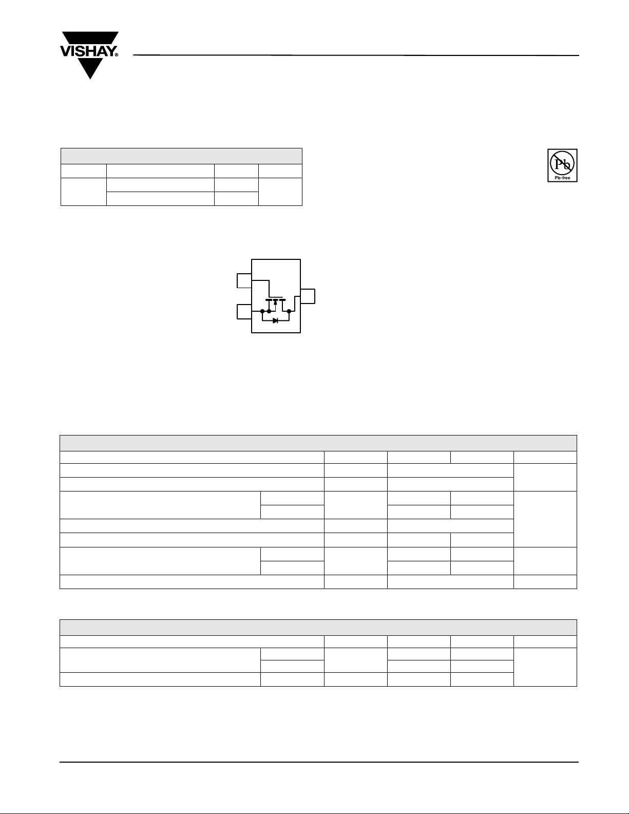
TO-236
(SOT-23)
G
1
D
3
S
2
Top View
Si2306BDS (L6 )*
* Marking Code
Ordering Information: Si2306BDS-T1-E3 (Lead (Pb)-free)
Si2306BDS-T1-GE3 (Lead (Pb)-free and Halogen-free)
ABSOLUTE MAXIMUM RATINGS TA = 25 °C, unless otherwise noted
Parameter Symbol 5 s Steady State Unit
Drain-Source Voltage
Gate-Source Voltage
Continuous Drain Current (T
= 150 °C)
J
a, b
Pulsed Drain Current
Continuous Source Current (Diode Conduction)
Maximum Power Dissipation
a, b
a, b
Operating Junction and Storage Temperature Range
TA = 25 °C
= 70 °C
T
A
TA = 25 °C
= 70 °C
T
A
V
DS
V
GS
I
D
I
DM
I
S
P
D
T
, T
J
stg
4.0 3.16
3.5 2.7
1.04 0.62
1.25 0.75
0.8 0.48
30
± 20
20
W
- 55 to 150 °C
V
A
THERMAL RESISTANCE RATINGS
Parameter Symbol Typical Maximum Unit
Maximum Junction-to-Ambient
a
Maximum Junction-to-Foot (Drain) Steady State
t ≤ 5 s
Steady State 130 166
R
thJA
R
thJF
Notes:
a. Surface Mounted on FR4 board, t ≤ 5 s.
b. Pulse width limited by maximum junction temperature.
c. Surface Mounted on FR4 board.
For SPICE model information via the Worldwide Web: http://www.vishay.com/www/product/spice.htm
Document Number: 73234
S-80642-Rev. B, 24-Mar-08
80 100
°C/W
60 75
www.vishay.com
1

Si2306BDS
Vishay Siliconix
SPECIFICATIONS TA = 25 °C, unless otherwise noted
Limits
Parameter Symbol Test Conditions
Min. Typ. Max.
Static
Drain-Source Breakdown Voltage
Gate-Threshold Voltage
Gate-Body Leakage
Zero Gate Voltage Drain Current
On-State Drain Current
Drain-Source On-Resistance
Forward Transconductance
a
a
a
Diode Forward Voltage
V
(BR)DSS
V
GS(th)
I
GSS
I
DSS
I
V
D(on)
R
DS(on)
g
fs
V
SD
VGS = 0 V, ID = 250 µA
V
= VGS, ID = 250 µA
DS
VDS = 0 V, VGS = ± 20 V
V
= 30 V, V
DS
V
= 30 V, V
DS
V
DS
V
GS
GS
= 0 V, TJ = 55 °C
GS
≥ 4.5 V, V
= 10 V, ID = 3.5 A
= 4.5 V, ID = 2.8 A
VDS = 4.5 V, ID = 2.5 A
IS = 1.25 A, V
GS
GS
GS
= 0 V
= 10 V
= 0 V
30
1.0 3.0
± 100 nA
0.5
10
6A
0.038 0.047
0.052 0.065
7.0 S
0.8 1.2 V
Dynamic
Gate Charge
Total Gate Charge
Gate-Source Charge
Gate-Drain Charge
Gate Resistance
Input Capacitance
Output Capacitance
Reverse Transfer Capacitance
Q
g
Q
gt
Q
gs
Q
gd
R
g
C
iss
C
oss
C
rss
VDS = 15 V, V
V
= 15 V, V
DS
= 5 V, ID = 2.5 A
GS
= 10 V, ID = 2.5 A
GS
f = 1.0 MHz
VDS = 15 V, VGS = 0 V, f = 1 MHz
3.0 4.5
69
1.6
0.6
2.557.5Ω
305
65
29
Switching
t
Tur n -O n De l ay Ti m e
Rise Time
Turn-Off Delay Time
Fall Time
Reverse Recovery Time
Body Diode Reverse Recovery Charge
d(on)
t
d(off)
Q
= 15 V, RL = 15 Ω
t
r
t
f
t
rr
rr
V
DD
I
≅ 1 A, V
D
= 10 V, Rg = 6 Ω
GEN
IF = 1.25 A, di/dt = 100 A/µs
711
12 18
14 25
610
14 21
610nC
Notes:
a. Pulse test: Pulse width ≤ 300 µs, duty cycle ≤ 2 %.
Stresses beyond those listed under “Absolute Maximum Ratings” may cause permanent damage to the device. These are stress ratings only, and functional operation
of the device at these or any other conditions beyond those indicated in the operational sections of the specifications is not implied. Exposure to absolute maximum
rating conditions for extended periods may affect device reliability.
Unit
V
µA
Ω
nC
pF
ns
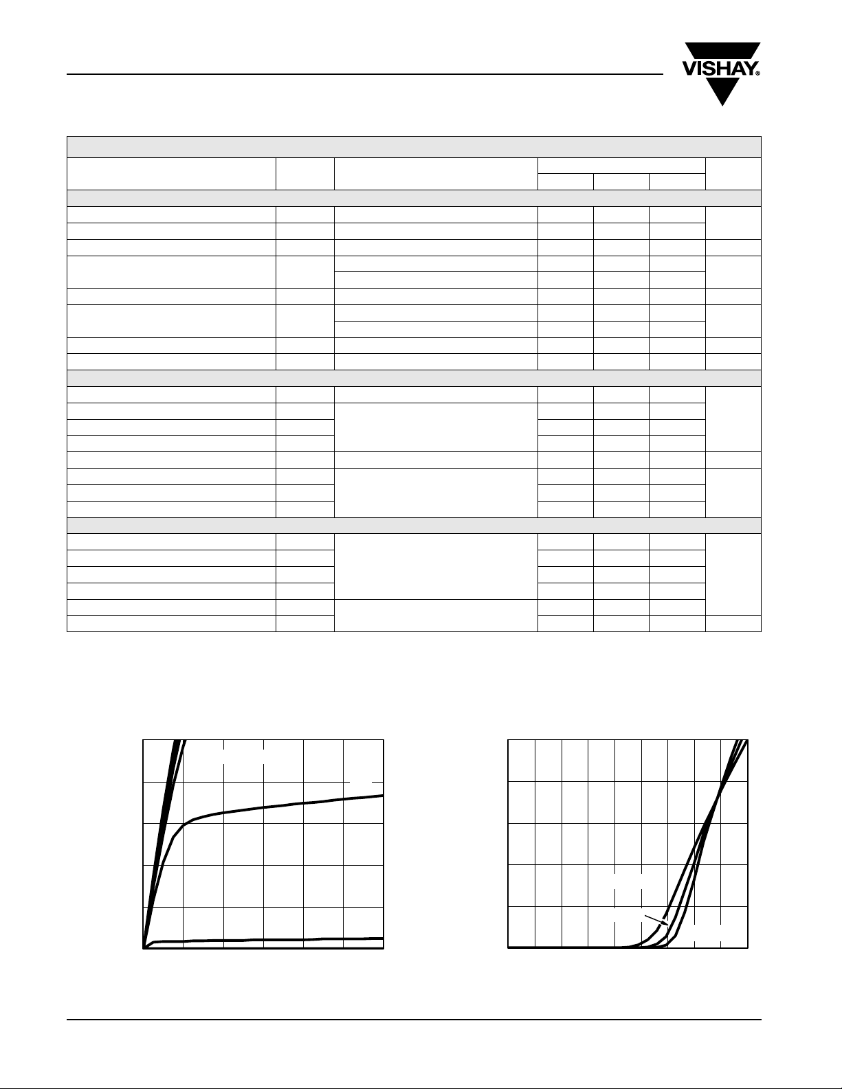
TYPICAL CHARACTERISTICS 25 °C, unless otherwise noted
20
VGS = 10 thru 5 V
16
12
8
Drain Current (A)I
-
D
4
0
www.vishay.com
2
0123456
- Drain-to-Source Voltage (V)
V
DS
Output Characteristics
4 V
- Drain Current (A)I
3 V
20
16
12
8
D
4
0
0.0 0.5 1.0 1.5 2.0 2.5 3.0 3.5 4.0 4.5
V
GS
TC = 125 °C
25 °C
- Gate-to-Source Voltage (V)
Transfer Characteristics
Document Number: 73234
S-80642-Rev. B, 24-Mar-08
- 55 °C
 Loading...