Vishay Si2304BDS Schematic [ru]

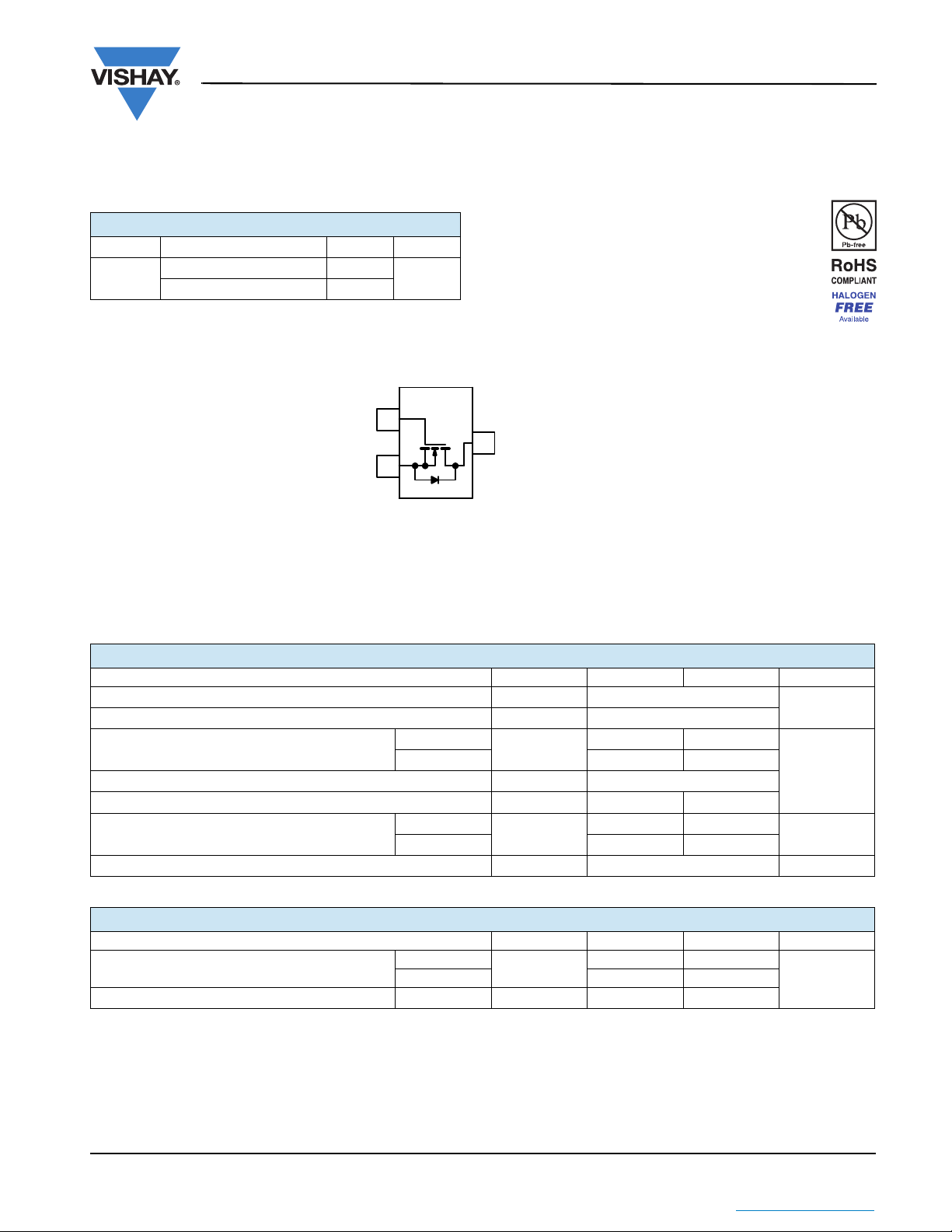
PRODUCT SUMMARY
Ordering Information: Si2304BDS-T1-E3 (Lead (Pb)-free)
Si2304BDS-T1-GE3 (Lead (Pb)-free and Halogen-free)
* Marking Code
Si2304BDS (L4)*
G
S
D
Top View
2
3
TO-236
(SOT-23)
1
VDS (V) R
30
0.070 at V
0.105 at V
()I
DS(on)
= 10 V
GS
= 4.5 V
GS
N-Channel 30 V (D-S) MOSFET
FEATURES
(A) Qg (Typ.)
D
3.2
2.6
2.6
• Halogen-free According to IEC 61249-2-21
Definition
• TrenchFET
•100 % R
®
Power MOSFET
Te s te d
g
• Compliant to RoHS Directive 2002/95/EC
Si2304BDS
Vishay Siliconix
ABSOLUTE MAXIMUM RATINGS (TA = 25 °C, unless otherwise noted)
Parameter Symbol 5 s Steady State Unit
Drain-Source Voltage
Gate-Source Voltage
Continuous Drain Current (T
= 150 °C)
J
a, b
Pulsed Drain Current
Continuous Source Current (Diode Conduction)
Maximum Power Dissipation
a, b
a, b
Operating Junction and Storage Temperature Range
TA = 25 °C
= 70 °C
T
A
TA = 25 °C
T
= 70 °C
A
V
DS
V
GS
I
D
I
DM
I
S
P
D
T
, T
J
stg
3.2 2.6
2.5 2.1
0.9 0.62
1.08 0.75
0.69 0.48
30
± 20
10
W
- 55 to 150 °C
V
A
THERMAL RESISTANCE RATINGS
Parameter Symbol Typical Maximum Unit
Maximum Junction-to-Ambient
Maximum Junction-to-Foot (Drain) Steady State
a
t 5 s
Steady State 130 166
R
thJA
R
thJF
Notes:
a. Surface mounted on FR4 board, t 5 s.
b. Pulse width limited by maximum junction temperature.
c. Surface mounted on FR4 board.
For SPICE model information via the Worldwide Web: http://www.vishay.com/www/product/spice.htm
90 115
°C/W
60 75
Document Number: 72503
S11-1908-Rev. E, 26-Sep-11
THE PRODUCTS DESCRIBED HEREIN AND THIS DOCUMENT ARE SUBJECT TO SPECIFIC DISCLAIMERS, SET FORTH AT www.vishay.com/doc?91000
This document is subject to change without notice.
www.vishay.com
1

Si2304BDS
0
2
4
6
8
10
0246810
VGS = 10 thru 5 V
V
DS
- Drain-to-Source Voltage (V)
- Drain Current (A)I
D
4 V
3 V
Vishay Siliconix
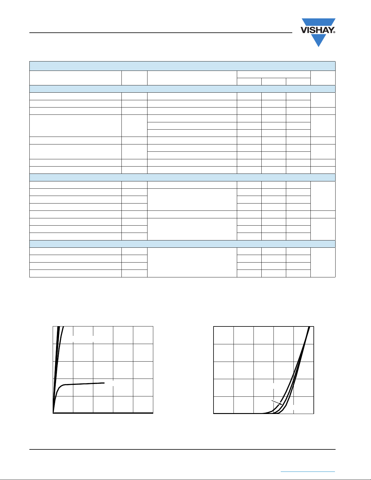
SPECIFICATIONS (TA = 25 °C, unless otherwise noted)
Limits
Parameter Symbol Test Conditions
Min. Typ. Max.
Static
Drain-Source Breakdown Voltage
Gate-Threshold Voltage
Gate-Body Leakage
Zero Gate Voltage Drain Current
On-State Drain Current
Drain-Source On-Resistance
Forward Transconductance
a
a
a
Diode Forward Voltage
V
(BR)DSS
V
GS(th)
I
GSS
I
DSS
I
V
D(on)
R
DS(on)
g
fs
V
SD
VGS = 0 V, ID = 250 µA
V
= VGS, ID = 250 µA
DS
VDS = 0 V, VGS = ± 20 V
V
= 30 V, V
DS
V
DS
V
DS
= 30 V, V
= 30 V, V
DS
V
GS
V
GS
= 0 V, TJ = 55 °C
GS
= 1 V, TJ = 25 °C
GS
4.5 V, V
= 10 V, ID = 2.5 A
= 4.5 V, ID = 2 A
VDS = 4.5 V, ID = 2.5 A
IS = 1.25 A, V
GS
GS
GS
= 0 V
= 10 V
= 0 V
30
1.5 3
± 100 nA
0.5
10
1
6A
0.055 0.070
0.080 0.105
6S
0.8 1.2 V
Dynamic
Gate Charge
Total Gate Charge
Gate-Source Charge
Gate-Drain Charge
Gate Resistance
Input Capacitance
Reverse Transfer Capacitance
Q
g
Q
gt
Q
gs
Q
gd
R
g
C
iss
C
oss
C
rss
VDS = 15 V, V
V
= 15 V, V
DS
VDS = 15 V, VGS = 0 V, f = 1 MHz
= 5 V, ID = 2.5 A
GS
2.6 4
4.6 7
= 10 V, ID = 2.5 A
GS
0.8
1.15
f = 1 MHz 0.6 3 6
225
50
28
Switching
Tur n -O n De l a y T im e
Rise Time
Turn-Off Delay Time
Fall Time
t
d(on)
t
d(off)
7.5 12
V
t
r
t
f
I
= 15 V, RL = 15
DD
1 A, V
D
= 10 V, Rg = 6
GEN
12.5 20
19 30
15 25
Notes:
a. Pulse test: PW 300 µs, duty cycle 2 %.
Stresses beyond those listed under “Absolute Maximum Ratings” may cause permanent damage to the de vice. These are stress rating s only, and functional operation
of the device at these or any other conditions beyond those indicated in the operational sections of the specifications is not implied. Exposure to absolute maximum
rating conditions for extended periods may affect device reliability.
Unit
V
µA
nC
pFOutput Capacitance
ns
TYPICAL CHARACTERISTICS (25 °C, unless otherwise noted)
www.vishay.com
2
THE PRODUCTS DESCRIBED HEREIN AND THIS DOCUMENT ARE SUBJECT TO SPECIFIC DISCLAIMERS, SET FORTH AT www.vishay.com/doc?91000
Output Characteristics
10
8
6
4
- Drain Current (A)I
D
2
0
012345
This document is subject to change without notice.
TC = 125 °C
25 °C
- Gate-to-Source Voltage (V)
V
GS
Transfer Characteristics
Document Number: 72503
S11-1908-Rev. E, 26-Sep-11
- 55 °C

TYPICAL CHARACTERISTICS (25 °C, unless otherwise noted)
0.0 0.2 0.4 0.6 0.8 1.0 1.2
TJ = 150 °C
TJ = 25 °C
10
0.001
V
SD
- Source-to-Drain Voltage (V)
- Source Current (A)I
S
0.01
0.1
1
0
50
100
150
200
250
300
350
0 5 10 15 20 25 30
VDS - Drain-to-Source Voltage (V)
C
rss
C
oss
C
iss
C - Capacitance (pF)
0.6
0.8
1.0
1.2
1.4
1.6
- 50 - 25 0 25 50 75 100 125 150
VGS = 10 V
I
D
= 2.5 A
T
J
- Junction Temperature (°C)
R
DS(on)
- On-Resistance (Normalized)
0.00
0.04
0.08
0.12
0.16
0.20
0246810
ID = 2.5 A
-R
DS(on)
VGS - Gate-to-Source Voltage (V)
0.24
0.20
0.16
0.12
-R
0.08
DS(on)
0.04
0.00
10
8
VGS = 4.5 V
VGS = 10 V
0246810
ID - Drain Current (A)
On-Resistance vs. Drain Current
VDS = 15 V
= 2.5 A
I
D
Si2304BDS
Vishay Siliconix
Capacitance
6
4
- Gate-to-Source Voltage (V)
GS
2
V
0
012345
Qg - Total Gate Charge (nC)
Gate Charge
On-Resistance vs. Junction Temperature
Document Number: 72503
S11-1908-Rev. E, 26-Sep-11
THE PRODUCTS DESCRIBED HEREIN AND THIS DOCUMENT ARE SUBJECT TO SPECIFIC DISCLAIMERS, SET FORTH AT www.vishay.com/doc?91000
Source-Drain Diode Forward Voltage
On-Resistance vs. Gate-to-Source Voltage
www.vishay.com
3
This document is subject to change without notice.
 Loading...