Vishay Si2302CDS Schematic [ru]

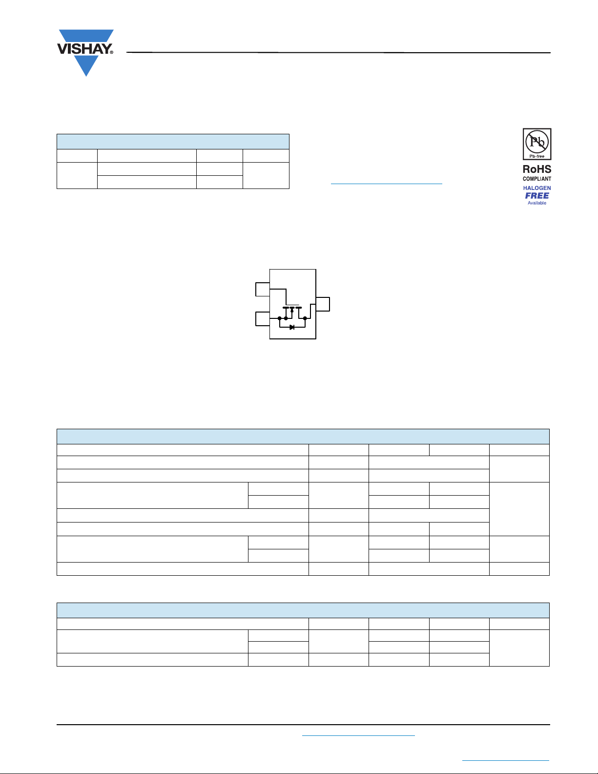
PRODUCT SUMMARY
Ordering Information: Si2302CDS-T1-E3 (Lead (Pb)-free)
Si2302CDS-T1-GE3 (Lead (Pb)-free and Halogen-free)
* Marking Code
Si2302CDS (N2)*
G
S
D
Top View
2
3
TO-236
(SOT-23)
1
VDS (V) R
20
0.057 at V
0.075 at V
()I
DS(on)
= 4.5 V
GS
= 2.5 V
GS
N-Channel 20 V (D-S) MOSFET
FEATURES
(A) Qg (Typ.)
D
2.9
2.6
3.5
• TrenchFET® Power MOSFET
• Material categorization:
For definitions of compliance please see
www.vishay.com/doc?99912
APPLICATIONS
• Load Switching for Portable Devices
• DC/DC Converter
Si2302CDS
Vishay Siliconix
ABSOLUTE MAXIMUM RATINGS (TA = 25 °C, unless otherwise noted)
Parameter Symbol 5 s Steady State Unit
Drain-Source Voltage
Gate-Source Voltage
Continuous Drain Current (T
Pulsed Drain Current
= 150 °C)
J
b
Continuous Source Current (Diode Conduction)
Power Dissipation
a
a
a
Operating Junction and Storage Temperature Range
THERMAL RESISTANCE RATINGS
Parameter Symbol Typical Maximum Unit
Maximum Junction-to-Ambient
Maximum Junction-to-Foot Steady State
Notes:
a. Surface mounted on 1" x 1" FR4 board.
b. Pulse width limited by maximum junction temperature.
Document Number: 68645
S12-2336-Rev. D, 01-Oct-12
THE PRODUCTS DESCRIBED HEREIN AND THIS DOCUMENT ARE SUBJECT TO SPECIFIC DISCLAIMERS, SET FORTH AT www.vishay.com/doc?91000
a
For technical questions, contact: pmostechsupport@vishay.comm
This document is subject to change without notice.
V
DS
V
GS
TA = 25 °C
T
= 70 °C
A
TA = 25 °C
= 70 °C
T
A
t 5 s
Steady State 140 175
I
D
I
DM
I
S
P
D
T
, T
J
stg
R
thJA
R
thJF
2.9 2.6
2.3 2.1
0.72 0.6
0.86 0.71
0.55 0.46
120 145
62 78
20
± 8
10
- 55 to 150 °C
V
A
W
°C/W
www.vishay.com
1

Si2302CDS
0
2
4
6
8
10
0.0 0.4 0.8 1.2 1.6 2.0
VGS- Gate-to-Source Voltage (V)
- Drain Current (A)I
D
TC= 25 °C
TC= 125 °C
TC= - 55 °C
Vishay Siliconix
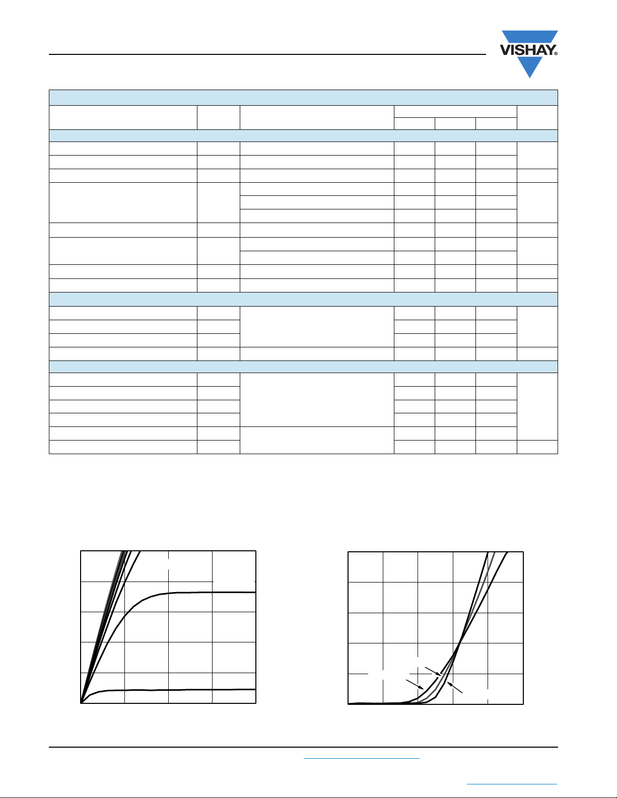
SPECIFICATIONS (TA = 25 °C, unless otherwise noted)
Limits
Parameter Symbol Test Conditions
Min. Typ. Max.
Static
Drain-Source Breakdown Voltage
Gate-Threshold Voltage
Gate-Body Leakage
Zero Gate Voltage Drain Current
On-State Drain Current
Drain-Source On-Resistance
Forward Transconductance
a
a
a
Diode Forward Voltage
Dynamic
b
Total Gate Charge
Gate-Drain Charge
Gate Resistance
V
DS
V
GS(th)
I
GSS
I
DSS
I
V
D(on)
R
DS(on)
g
fs
V
SD
Q
g
Q
gs
Q
gd
R
g
VGS = 0 V, ID = 250 µA
V
= VGS, ID = 250 µA
DS
VDS = 0 V, VGS = ± 8 V
V
= 20 V, V
DS
V
= 20 V, V
DS
V
DS
= 20 V, V
GS
GS
10 V, V
DS
V
= 4.5 V, ID = 3.6 A
GS
V
= 2.5 V, ID = 3.1 A
GS
VDS = 5 V, ID = 3.6 A
IS = 0.95 A, V
V
= 10 V, V
DS
GS
f = 1 MHz 2 4 8
= 0 V
GS
= 0 V, TJ = 50 °C
= 0 V, TJ = 70 °C
= 4.5 V
GS
= 0 V
GS
= 4.5 V, ID = 3.6 A
20
0.40 0.85
± 100 nA
0.1
4
15
6A
0.045 0.057
0.056 0.075
13 S
0.7 1.2 V
3.5 5.5
0.6
0.45
Switching
Tur n -O n De l a y T i m e
Rise Time
Turn-Off Delay Time
Fall Time
Source-Drain Reverse Recovery Time
Body Diode Reverse Recovery Charge
t
d(on)
t
d(off)
Q
t
r
t
f
t
rr
rr
V
= 10 V, RL = 2.78
DD
3.6 A, V
I
D
= 4.5 V, Rg = 1
GEN
IF = 3.6 A, dI/dt = 100 A/µs
815
715
30 45
715
8.5 15
24nC
Notes:
a. Pulse test: Pulse width 300 µs, duty cycle 2 %.
b. Guaranteed by design, not subject to production testing.
Stresses beyond those listed under “Absolute Maximum Ratings” may cause permanent damage to the device. These are stress ratings only, and functional operation
of the device at these or any other conditions beyond those indicated in the operational sections of the specifications is not implied. Exposure to absolute maximum
rating conditions for extended periods may affect device reliability.
Unit
V
µA
nCGate-Source Charge
ns
TYPICAL CHARACTERISTICS (25 °C, unless otherwise noted)
10
VGS=5V thru 2 V
8
6
4
- Drain Current (A)I
D
2
0
0.0 0.5 1.0 1.5 2.0
www.vishay.com
2
VDS- Drain-to-Source Voltage (V)
Output Characteristics
THE PRODUCTS DESCRIBED HEREIN AND THIS DOCUMENT ARE SUBJECT TO SPECIFIC DISCLAIMERS, SET FORTH AT www.vishay.com/doc?91000
VGS=1.5V
VGS=1V
Transfer Characteristics
For technical questions, contact: pmostechsupport@vishay.comm
This document is subject to change without notice.
Document Number: 68645
S12-2336-Rev. D, 01-Oct-12

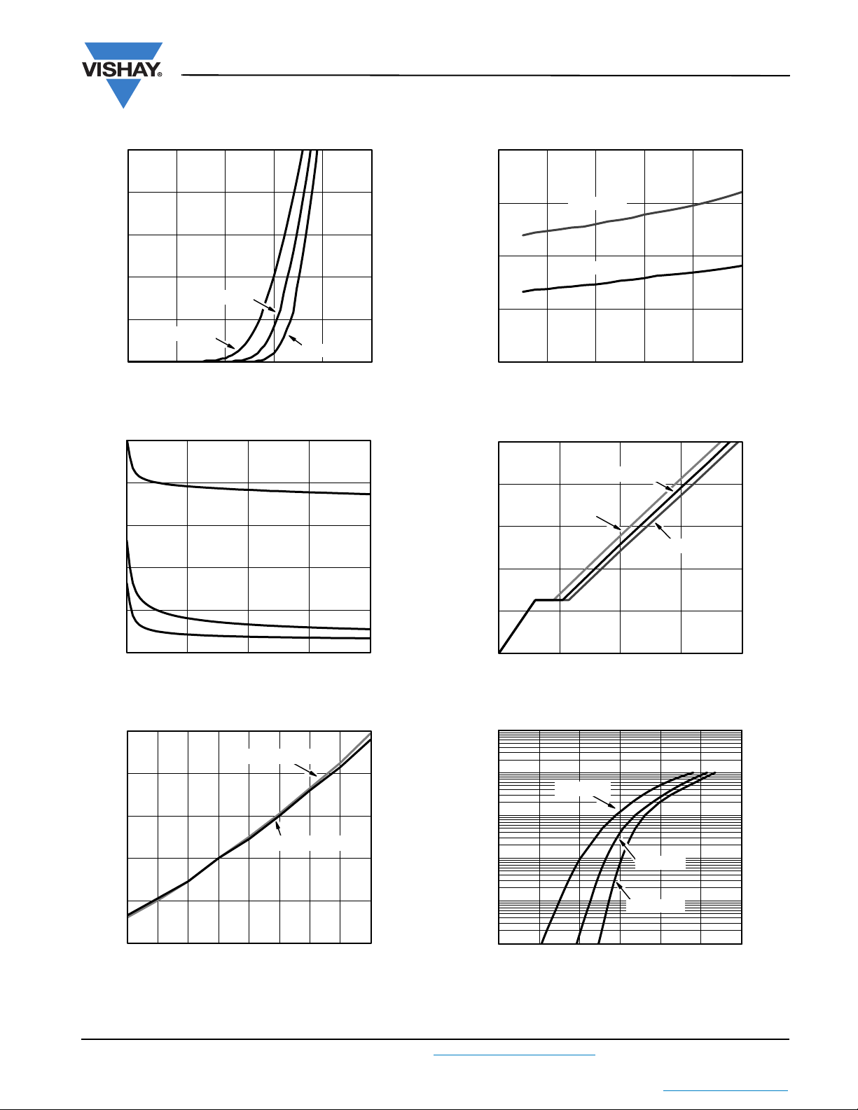
TYPICAL CHARACTERISTICS (25 °C, unless otherwise noted)
0
80
160
240
320
400
0 5 10 15 20
C
iss
VDS- Drain-to-Source Voltage (V)
C - Capacitance (pF)
C
oss
C
rss
0.6
0.8
1.0
1.2
1.4
1.6
- 50 - 25 0 25 50 75 100 125 150
TJ-Junction Temperature (°C)
(Normalized)
- On-Resistance
R
DS(on)
VGS=2.5V,ID=3.1A
VGS=4.5V,ID=3.6A
0.03
0.04
0.05
0.06
0.07
02468 10
- On-Resistance (Ω)R
DS(on)
ID- Drain Current (A)
VGS=2.5V
VGS=4.5V
2.0
1.6
1.2
0.8
- Drain Current (A)I
D
0.4
TC= 125 °C
0.0
0.0 0.3 0.6 0.9 1.2 1.5
TC= 25 °C
TC= - 55 °C
VGS- Gate-to-Source Voltage (V)
Si2302CDS
Vishay Siliconix
Transfer Characteristics
Capacitance
On-Resistance vs. Drain Current
5
ID=3.6A
4
3
2
- Gate-to-Source Voltage (V)
GS
1
V
0
01234
Qg- Total Gate Charge (nC)
VDS=10V
VDS= 5 V
VDS= 15 V
Gate Charge
100
10
TJ= 150 °C
1
Document Number: 68645
S12-2336-Rev. D, 01-Oct-12
THE PRODUCTS DESCRIBED HEREIN AND THIS DOCUMENT ARE SUBJECT TO SPECIFIC DISCLAIMERS, SET FORTH AT www.vishay.com/doc?91000
On-Resistance vs. Junction Temperature
0.1
- Source Current (A)I
S
0.01
0.001
0.0 0.2 0.4 0.6 0.8 1.0 1.2
VSD-Source-to-Drain Voltage (V)
Source-Drain Diode Forward Voltage
For technical questions, contact: pmostechsupport@vishay.comm
This document is subject to change without notice.
TJ= 25 °C
TJ= - 55 °C
www.vishay.com
3
 Loading...