

i179076
1
2
E
C
A
C
15
16
3
4
E
C
A
C
13
14
5
6
E
C
A
C
11
12
7
8
E
C
A
C
9
10
查询SFH6916供应商查询SFH6916供应商
VISHAY
SFH6916
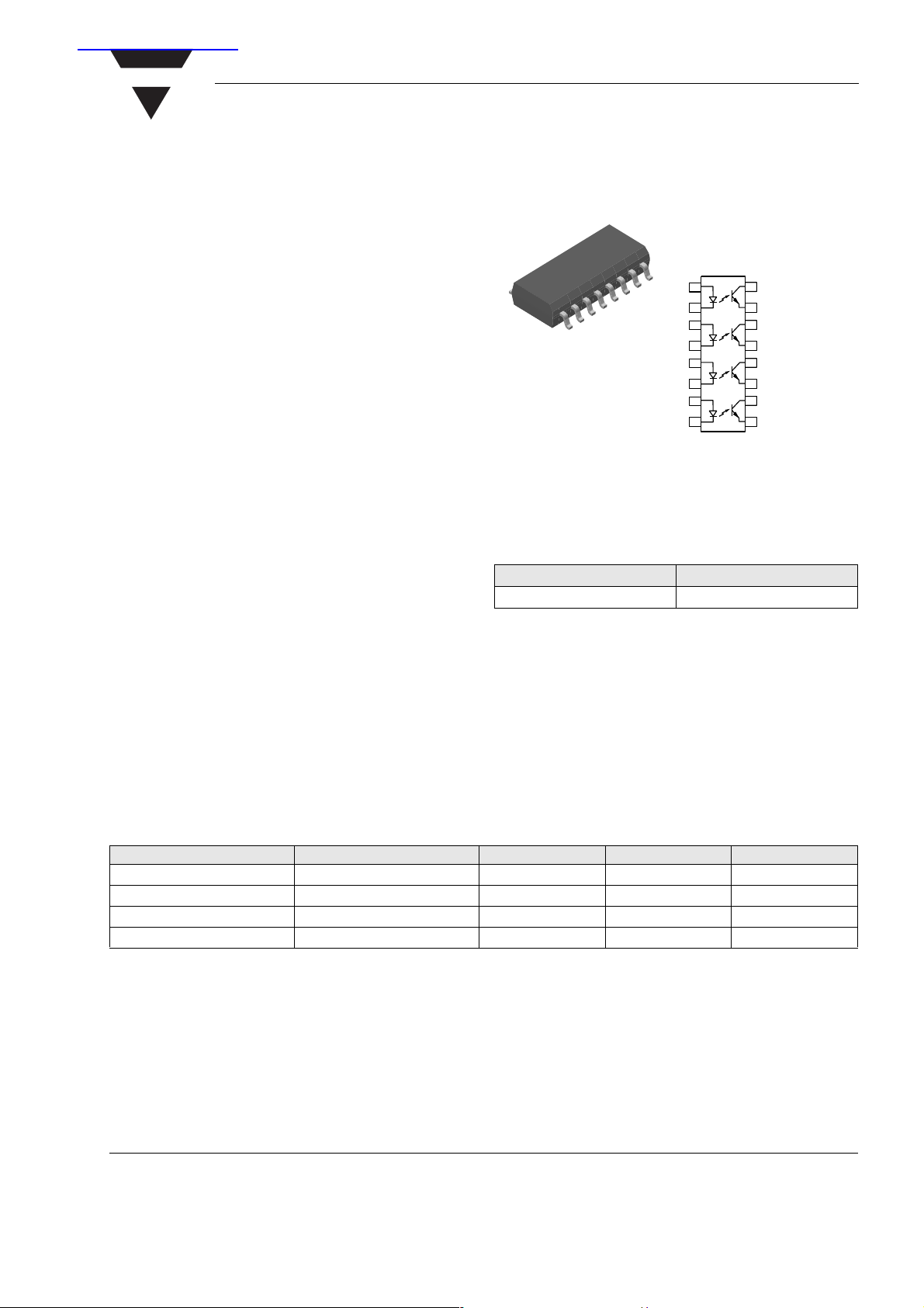
Vishay Semiconductors
Optocoupler, Phototransistor Output, Quad Channel, SOP-16,
Half Pitch Mini-Flat Package
Features
• SOP (Small Outline Package)
• Isolation Test Voltage, 3750 V
• High Collector-Emitter Voltage,
V
= 70 V
CEO
• Low Saturation Voltage
• Fast Switching Times
• Temperature Stable
• Low Coupling Capacitance
• End-Stackable, 0.050 " (1.27 mm) Spacing
Agency Approvals
• UL File #E52744 System Code U
RMS
(1.0 s)
The coupling devices are designed for signal transmission between two electrically separated circuits.
Description
The SFH6916 has a GaAs infrared emitter, which is
optically coupled to a silicon planar phototransistor
detector, and is incorporated in a 16-pin 50 mil lead
pitch miniflat package. It features a high current transfer ratio, low coupling capacitance, and high isolation
Order Information
Part Remarks
SFH6916 CTR 50 - 300 %, SMD-16
For additional information on the available options refer to
Option Information.
voltage.
Absolute Maximum Ratings
T
= 25 °C, unless otherwise specified
amb
Stresses in excess of the absolute Maximum Ratings can cause permanent damage to the device. Functional operation of the device is
not implied at these or any other conditions in excess of those given in the operational sections of this document. Exposure to absolute
Maximum Rating for extended periods of the time can adversely affect reliability.
Input
Parameter Test condition Symbol Value Unit
Reverse voltage V
DC Forward current I
Surge forward current t
Total power dissipation P
≤ 10 µsI
p
R
F
FSM
diss
6.0 V
50 mA
2.5 A
80 mW
Document Number 83687
Rev. 1.4, 20-Apr-04
www.vishay.com
1
SFH6916
VISHAY
Vishay Semiconductors
Output
Parameter Test condition Symbol Val ue Unit
Collector-emitter voltage V
Emitter-collector voltage V
Collector current I
t
≤ 1.0 ms I
p
Total power dissipation per
CE
EC
C
C
P
diss
70 V
7.0 V
50 mA
100 mA
150 mW
channel
Coupler
Parameter Test condition Symbol Val ue Unit
Isolation test voltage between
V
ISO
emitter and detector (1.0 s)
Creepage ≥ 5.33 mm
Clearance ≥ 5.08 mm
Comparative tracking index per
DIN IEC 112/VDEo 303, part 1
Isolation resistance V
= 500 V, T
IO
= 500 V, T
V
IO
Storage temperature range T
Ambient temperature range T
Junction temperature T
= 25 °C R
amb
= 100 °C R
amb
IO
IO
stg
amb
j
Soldering temperature max. 10 s dip soldering distance
to seating plane ≥ 1.5 mm
Total power dissipation P
tot
3750 V
≥ 175
12
≥ 10
11
≥ 10
- 55 to + 125 °C
- 55 to +100 °C
100 °C
260 °C
70 mW
RMS
Ω
Ω
Electrical Characteristics
T
= 25 °C, unless otherwise specified
amb
Minimum and maximum values are testing requirements. Typical values are characteristics of the device and are the result of engineering
evaluation. Typical values are for information only and are not part of the testing requirements.
Input
T
= 25 °C (except where noted)
amb
Parameter Test condition Symbol Min Ty p. Max Unit
Forward voltage I
Reverse current V
Capacitance C
= 5 mA V
F
= 6.0 V I
R
O
Thermal resistance R
F
R
C
O
thja
1.15 1.4 V
0.01 10 µA
14 pF
1000 K/W
Output
Parameter Test condition Symbol Min Ty p. Max Unit
Collector-emitter leakage
current
Collector-emitter capacitance V
= 20 V I
V
CE
= 5.0 V, f = 1.0 MHz C
CE
Thermal resistance R
CEO
CE
thja
2.8 pF
500 K/W
100 nA
www.vishay.com
2
Document Number 83687
Rev. 1.4, 20-Apr-04
VISHAY
isfh6916_02
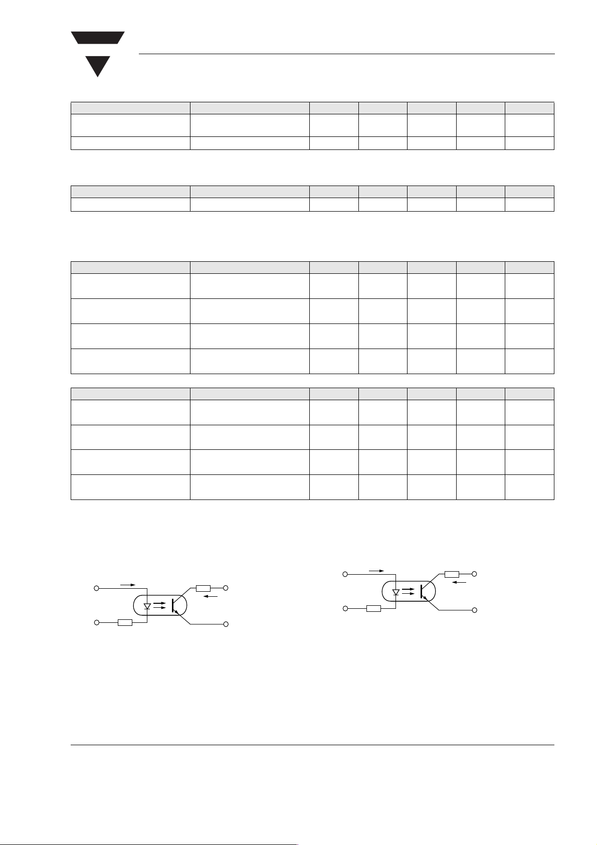
RL=1.9 kΩ
V
CC
=5V
I
C
50 Ω
I
F
Coupler
Parameter Test condition Symbol Min Ty p. Max Unit
Collector-emitter saturation
voltage
Coupling capacitance f = 1.0 MHz C
Current Transfer Ratio
Parameter Test condition Symbol Min Ty p. Max Unit
Current Transfer Ratio I
Switching Characteristics
Switching Operation (without saturation)
Parameter Test condition Symbol Min Ty p. Max Unit
Rise time I
Fall tim e I
Turn on time I
Turn off time I
Switching Operation (with saturation)
Parameter Test condition Symbol Min Ty p. Max Unit
Rise time I
Fall tim e I
Turn on time I
Turn off time I
= 20 mA, IC = 1.0 mA V
I
F
= 5.0 mA, VCC = 5.0 V CTR 50 300 %
F
= 2.0 mA, VCC = 10 V,
C
R
= 100 Ω
L
= 2.0 mA, VCC = 10 V,
C
= 100 Ω
R
L
= 2.0 mA, VCC = 10 V,
C
R
= 100 Ω
L
= 2.0 mA, VCC = 10 V,
C
= 100 Ω
R
L
= 16.0 mA, VCC = 5.0 V,
F
R
= 1.9 kΩ
L
= 16.0 mA, VCC = 5.0 V,
F
= 1.9 kΩ
R
L
= 16.0 mA, VCC = 5.0 V,
F
= 1.9 kΩ
R
L
= 16.0 mA, VCC = 5.0 V,
F
= 1.9 kΩ
R
L
CESAT
C
t
r
t
f
t
on
t
off
t
r
t
f
t
on
t
off
SFH6916
Vishay Semiconductors
0.1 0.4 V
1.0 pF
4.0 µs
3.0 µs
5.0 µs
4.0 µs
15 µs
0.5 µs
1.0 µs
30 µs
I
F
50 Ω
isfh6916_01
Fig. 1 Switching Operation (without Saturation)
Document Number 83687
Rev. 1.4, 20-Apr-04
RL=100 Ω
I
C
V
CC
=10V
Fig. 2 Switching Operation (with Saturation)
www.vishay.com
3

SFH6916
isfh6916_06
Collector Current (mA)
Collector-emitter Saturation Voltage, VCE(sat) (V)
100.000
10.000
1.000
0.100
0.010
0.001
0.0 0.2 0.4 0.6 0.8 1.0
IF=25mA
IF=10mA
IF= 5.0 mA
IF= 2.0 mA
IF= 1.0 mA
isfh6916_07
Normalized Output Current, CTR
1.4
1.2
1.0
0.8
0.6
0.4
0.2
0.0
Ambient Temperature, TA(°C)
–60 –40 –20 0 20 40 60 80 100
Normalized to 1.0 at TA=25°C
IF= 1.0 mA, VCE= 5.0 V
isfh6916_08
Ambient Temperature, TA(°C)
Normalized Output Current, CTR
1.2
1.0
0.8
0.6
0.4
0.2
0.0
–60 –40 –20 0 20 40 60 80 100
Normalized to 1.0 at TA=25°C
IF= 1.0 mA, VCE= 5.0 V
Vishay Semiconductors
VISHAY
Typical Characteristics (T
1.6
(V)
1.4
F
1.1
0.9
Forward Voltage, V
0.6
0.01 0.10 1.00 10.00 100.00
isfh6916_03
T = –25°C
T = –25°C
T=0°C
Forward Current, IF(mA)
= 25 °C unless otherwise specified)
amb
T = 100°C
T=75°C
T=50°C
T=25°C
Fig. 3 Diode Forward Voltage vs. Forward Current
80
70
(mA)
60
C
50
40
30
20
Collector Current, I
10
0
02 46810
isfh6916_04
IF=30mA
IF=20mA
IF=15mA
IF=10mA
IF=5mA
Collector to Emitter Voltage, VCE(V)
Fig. 6 Collector Current vs. Collector-Emitter Saturation Voltage
Fig. 4 Collector Current vs. Collector Emitter Voltage
1000.0
(nA)
CEO
100.0
10.0
1.0
–60 –40 –20 0 20 40 60 80 100
Collector to Emitter Dark Current, I
isfh6916_05
Fig. 5 Collector to Emitter Dark Current vs. Ambient Temperature
www.vishay.com
4
Ambient Temperature, TA(°C)
Fig. 7 Normalized Output Current vs. Ambient Temperature
24 V
40 V
12 V
Fig. 8 Normalized Output Current vs. Ambient Temperature
Document Number 83687
Rev. 1.4, 20-Apr-04

VISHAY
isfh6916_12
t
off
t
r
t
pdon
t
on
t
d
t
f
10%
50%
90%
Output
Input
10%
50%
90%
t
s
t
pdoff
300
VCE= 5.0 V
250
200
SFH6916
Vishay Semiconductors
Typical for
CTR=250%
150
100
50
Current Transfer Ratio, CTR (%)
0
0.1 1.0 10.0 50 100.0
isfh6916_09
Forward Current, IF(mA)
Typical for
CTR=150%
Fig. 9 Current Transfer Ratio vs. Forward Current
100.0
ton
10.0
1.0
Switching Time, (µ s)
0.1
0 500 1000 1500 2000
isfh6916_10
Load Resistance, RL(ohm)
toff
td
ts
VCC= 5.0 V
IC= 2.0 mA
Fig. 12 Switching Time Measurement
Fig. 10 Switching Time vs. Load Resistance
1000
IF= 5.0 mA
VCC= 5.0 V
TA=25°C
100
CTR = 150%
10
Switching Time, (µs)
1
0
100 1000 10000 100000
isfh6916_11
Load Resistance, RL(Ω)
Fig. 11 Switching Time vs. Load Resistance
Document Number 83687
Rev. 1.4, 20-Apr-04
t
f
t
s
t
r
t
d
www.vishay.com
5

SFH6916
Vishay Semiconductors
Package Dimensions in Inches (mm)
0.19 (4.83)
0.17 (4.32)
0.434 (11.02)
0.414 (10.52)
ISO Method A
0.080 (2.03)
0.075 (1.91)
0.034 (0.87)
0.024 (0.61)
.050 (1.27)
0.017 (0.43)
0.013 (0.33)
0.008 (0.20)
0.004 (0.10)
R .010 (.25)
.200 (5.08)
.290 (7.37)
0.220 (5.59)
0.200 (5.08)
40°
VISHAY
.014 (.36)
.036 (.91)
.045 (1.14)
10°
i178043
0.018 (0.46)
0.014 (0.36)
0.055 (1.40)
0.045 (1.14)
0.000 (0.00)
0.005 (0.13)
0.200 (5.08)
0.220 (5.59)
0.280 (7.11)
0.260 (6.60)
www.vishay.com
6
Document Number 83687
Rev. 1.4, 20-Apr-04

VISHAY
SFH6916
Vishay Semiconductors
Ozone Depleting Substances Policy Statement
It is the policy of Vishay Semiconductor GmbH to
1. Meet all present and future national and international statutory requirements.
2. Regularly and continuously improve the performance of our products, processes, distribution and
operatingsystems with respect to their impact on the health and safety of our employees and the public, as
well as their impact on the environment.
It is particular concern to control or eliminate releases of those substances into the atmosphere which are
known as ozone depleting substances (ODSs).
The Montreal Protocol (1987) and its London Amendments (1990) intend to severely restrict the use of ODSs
and forbid their use within the next ten years. Various national and international initiatives are pressing for an
earlier ban on these substances.
Vishay Semiconductor GmbH has been able to use its policy of continuous improvements to eliminate the
use of ODSs listed in the following documents.
1. Annex A, B and list of transitional substances of the Montreal Protocol and the London Amendments
respectively
2. Class I and II ozone depleting substances in the Clean Air Act Amendments of 1990 by the Environmental
Protection Agency (EPA) in the USA
3. Council Decision 88/540/EEC and 91/690/EEC Annex A, B and C (transitional substances) respectively.
Vishay Semiconductor GmbH can certify that our semiconductors are not manufactured with ozone depleting
substances and do not contain such substances.
We reserve the right to make changes to improve technical design
and may do so without further notice.
Parameters can vary in different applications. All operating parameters must be validated for each
customer application by the customer. Should the buyer use Vishay Semiconductors products for any
unintended or unauthorized application, the buyer shall indemnify Vishay Semiconductors against all
claims, costs, damages, and expenses, arising out of, directly or indirectly, any claim of personal
damage, injury or death associated with such unintended or unauthorized use.
Vishay Semiconductor GmbH, P.O.B. 3535, D-74025 Heilbronn, Germany
Telephone: 49 (0)7131 67 2831, Fax number: 49 (0)7131 67 2423
Document Number 83687
Rev. 1.4, 20-Apr-04
www.vishay.com
7
 Loading...