

Page 1
B-43
PRODUCT SUMMARY
I
F(AV)
Vishay High Power Products
Fast Recovery Diodes
(Hockey PUK Version), 810/910 A
FEATURES
• High power FAST recovery diode series
• 2.0 to 3.0 µs recovery time
• High voltage ratings up to 2500 V
• High current capability
• Optimized turn-on and turn-off characteristics
• Low forward recovery
• Fast and soft reverse recovery
• Press PUK encapsulation
• Hockey PUK version case style B-43
• Maximum junction temperature 150 °C
• Lead (Pb)-free
• Designed and qualified for industrial level
810/910 A
TYPICAL APPLICATIONS
• Snubber diode for GTO
• High voltage freewheeling diode
• Fast recovery rectifier applications
SD823C..C Series
RoHS
COMPLIANT
MAJOR RATINGS AND CHARACTERISTICS
PARAMETER TEST CONDITIONS
I
F(AV)
I
F(RMS)
I
FSM
V
RRM
t
rr
T
J
T
hs
50 Hz 9300 9600
60 Hz 9730 10 050
Range 1200 to 2500 1200 to 2500 V
T
J
ELECTRICAL SPECIFICATIONS
VOLTAGE RATINGS
V
, MAXIMUM REPETITIVE PEAK
TYPE NUMBER
SD823C..C
VOLTAGE
CODE
12 1200 1300
16 1600 1700
20 2000 2100
25 2500 2600
RRM
REVERSE VOLTAGE
V
SD823C..C
S20 S30
810 910 A
55 55 °C
1500 1690
2.0 3.0 µs
25
- 40 to 150
V
, MAXIMUM NON-REPETITIVE
RSM
PEAK REVERSE VOLTAGE
V
AT T
I
RRM
J
UNITS
A
°C
MAXIMUM
= TJ MAXIMUM
mA
50
Document Number: 93181 For technical questions, contact: ind-modules@vishay.com
Revision: 14-May-08 1
www.vishay.com
Page 2
SD823C..C Series
Vishay High Power Products
Fast Recovery Diodes
(Hockey PUK Version),
810/910 A
FORWARD CONDUCTION
PARAMETER SYMBOL TEST CONDITIONS
Maximum average forward current
at heatsink temperature
Maximum RMS forward current I
Maximum peak, one-cycle forward,
non-repetitive current
Maximum I
Maximum I
2
t for fusing I2t
2
√t for fusing I2√t t = 0.1 to 10 ms, no voltage reapplied 4320 4600 kA2√s
Low level value of threshold voltage V
High level value of threshold voltage V
Low level value of forward
slope resistance
High level value of forward
slope resistance
Maximum forward voltage drop V
I
F(AV)
F(RMS)
I
FSM
F(TO)1
F(TO)2
r
r
180° conduction, half sine wave
Double side (single side) cooled
25 °C heatsink temperature double side cooled 1500 1690
t = 10 ms
t = 8.3 ms 9730 10 050
t = 10 ms
t = 8.3 ms 8190 8450
t = 10 ms
t = 8.3 ms 395 420
t = 10 ms
t = 8.3 ms 279 297
(16.7 % x π x I
(I > π x I
(16.7 % x π x I
f1
(I > π x I
f2
Ipk = 1500 A, TJ = TJ maximum
FM
t
= 10 ms sinusoidal wave
p
No voltage
reapplied
100 % V
RRM
reapplied
No voltage
Sinusoidal half wave,
initial T
reapplied
100 % V
RRM
reapplied
< I < π x I
F(AV)
), TJ = TJ maximum 1.11 1.06
F(AV)
< I < π x I
F(AV)
), TJ = TJ maximum 0.76 0.57
F(AV)
F(AV)
F(AV)
SD823C..C
S20 S30
810 (425) 910 (470) A
55 (85) 55 (85) °C
9300 9600
7820 8070
= TJ maximum
J
432 460
306 326
), TJ = TJ maximum 1.00 0.95
), TJ = TJ maximum 0.80 0.60
2.20 1.85 V
UNITS
A
2
kA
V
mΩ
s
RECOVERY CHARACTERISTICS
TYPICAL VALUES
AT TJ = 125 °C
AT 25 % I
(µs)
RRM
Q
(µC)
rr
3.5 240 110
I
(A)
I
FM
t
rr
dir
rr
t
dt
I
RM(REC)
Q
rr
CODE
MAXIMUM VALUE
= 25 °C
AT T
J
AT 25 % I
t
rr
RRM
(µs)
TEST CONDITIONS
I
pk
SQUARE
PULSE
dI/dt
(A/µs)
V
(V)
t
r
rr
(A)
S20 2.0
S30 3.0 5.0 380 130
1000 50 - 50
THERMAL AND MECHANICAL SPECIFICATIONS
PARAMETER SYMBOL TEST CONDITIONS VALUES UNITS
Maximum junction operating and storage
temperature range
Maximum thermal resistance,
case junction to heatsink
Mounting force, ± 10 % 9800 (1000) N (kg)
Approximate weight 83 g
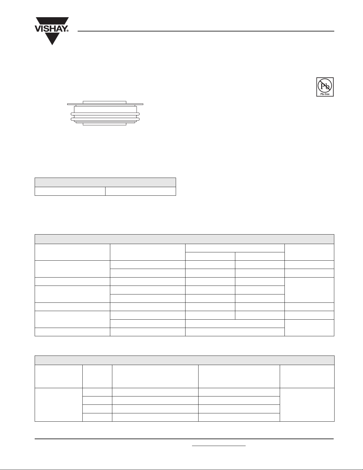
Case style See dimensions - link at the end of datasheet B-43
www.vishay.com For technical questions, contact: ind-modules@vishay.com
2 Revision: 14-May-08
T
R
, T
J
thJ-hs
Stg
DC operation single side cooled 0.076
DC operation double side cooled 0.038
- 40 to 150 °C
K/W
Document Number: 93181
Page 3
SD823C..C Series
Fast Recovery Diodes
(Hockey PUK Version),
ΔR
CONDUCTION ANGLE
Note
• The table above shows the increment of thermal resistance R
CONDUCTION
thJ-hs
SINUSOIDAL CONDUCTION RECTANGULAR CONDUCTION
SINGLE SIDE DOUBLE SIDE SINGLE SIDE DOUBLE SIDE
180° 0.007 0.007 0.005 0.005
120° 0.008 0.008 0.008 0.008
90° 0.010 0.010 0.011 0.011
60° 0.015 0.015 0.016 0.016
30° 0.026 0.026 0.026 0.026
160
140
120
100
SD823C..S20C Serie s
(Single Side Cooled)
R (DC) = 0.076 K/ W
thJ-hs
Cond uction Angle
Vishay High Power Products
810/910 A
TEST CONDITIONS UNITS
T
= TJ maximum K/W
J
when devices operate at different conduction angles than DC
thJ-hs
160
140
120
100
SD 8 2 3C . . S30 C Se r i e s
(Single Side Cooled)
R ( DC) = 0.076 K/W
thJ-hs
Cond uction Ang le
80
60
40
20
0 100 200 300 400 500 600 700
Maximum Allowable Heatsink Temperature (°C)
30°
Average Forward Current (A)
60°
90°
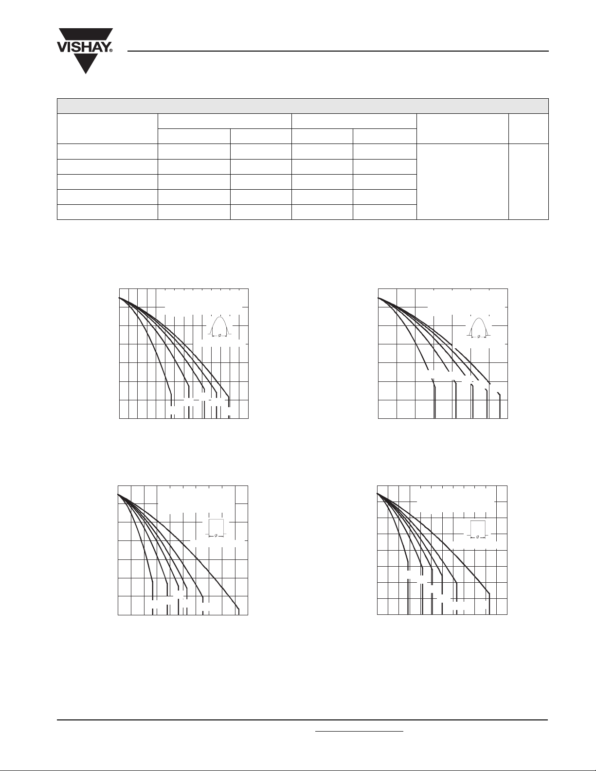
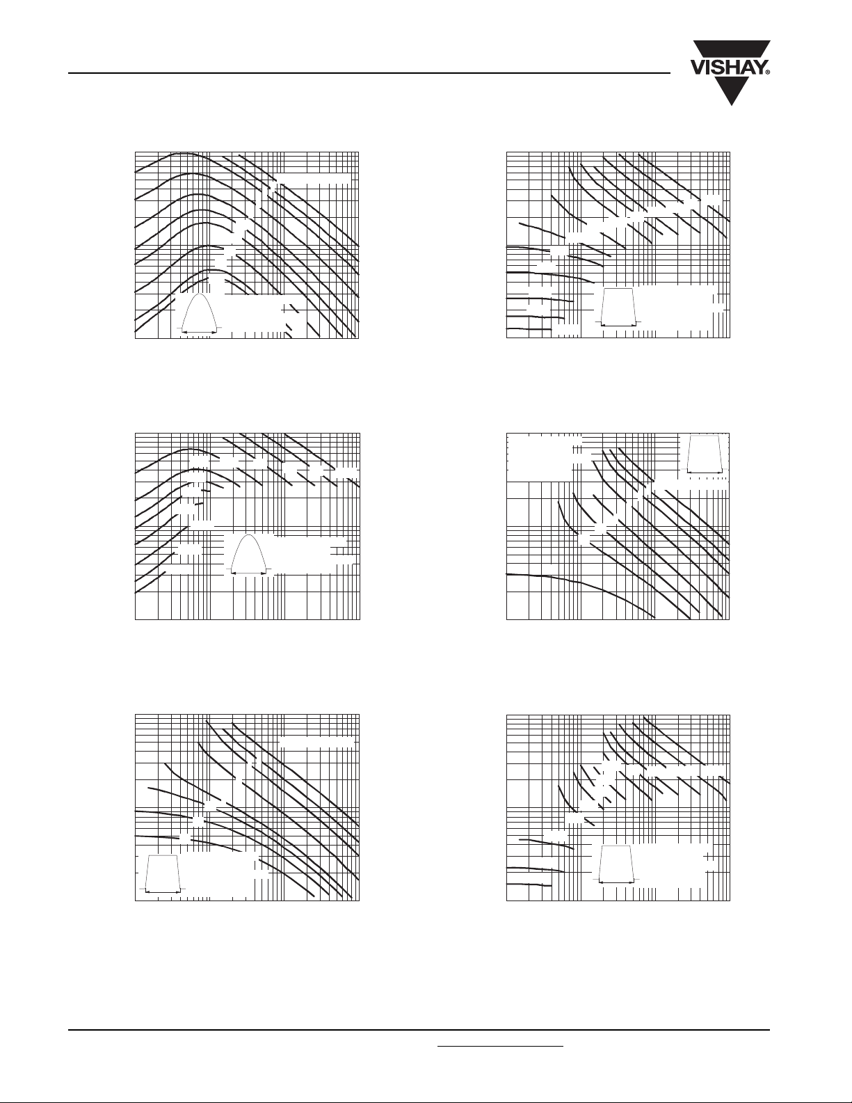
Fig. 1 - Current Ratings Characteristics
160
140
120
100
80
60
40
20
0 200 400 600 800 1000
Maximum Allowable Heat sink Temperature (°C)
SD823C..S20C Series
(Single Side Cooled)
R (DC) = 0.076 K/ W
thJ-hs
Cond uc tion Period
90°
60°
30°
Average Forward Current (A)
120°
180°
Fig. 2 - Current Ratings Characteristics
120°
180°
DC
80
30°
60°
60
40
20
0 100 200 300 400 500 600 700
Maximum Allowa ble Hea tsink Temperature (°C)
Average Forward Current (A)
90°
Fig. 3 - Current Ratings Characteristics
160
140
120
100
80
60
40
20
0
0 200 400 600 800 1000 1200
Maximum Allowable Heatsink Temperature (°C)
SD823C ..S30C Serie s
(Single Side Cooled)
R (DC) = 0.076 K/ W
thJ-hs
Conduction Period
30°
60°
90°
120°
180°
Average Forward Current (A)
Fig. 4 - Current Ratings Characteristics
120°
DC
180°
Document Number: 93181 For technical questions, contact: ind-modules@vishay.com
www.vishay.com
Revision: 14-May-08 3
Page 4
SD823C..C Series
Vishay High Power Products
160
140
120
100
80
60
40
20
0
0 200 400 600 800 1000
Maximum Allowable Heatsink Temperature (°C)
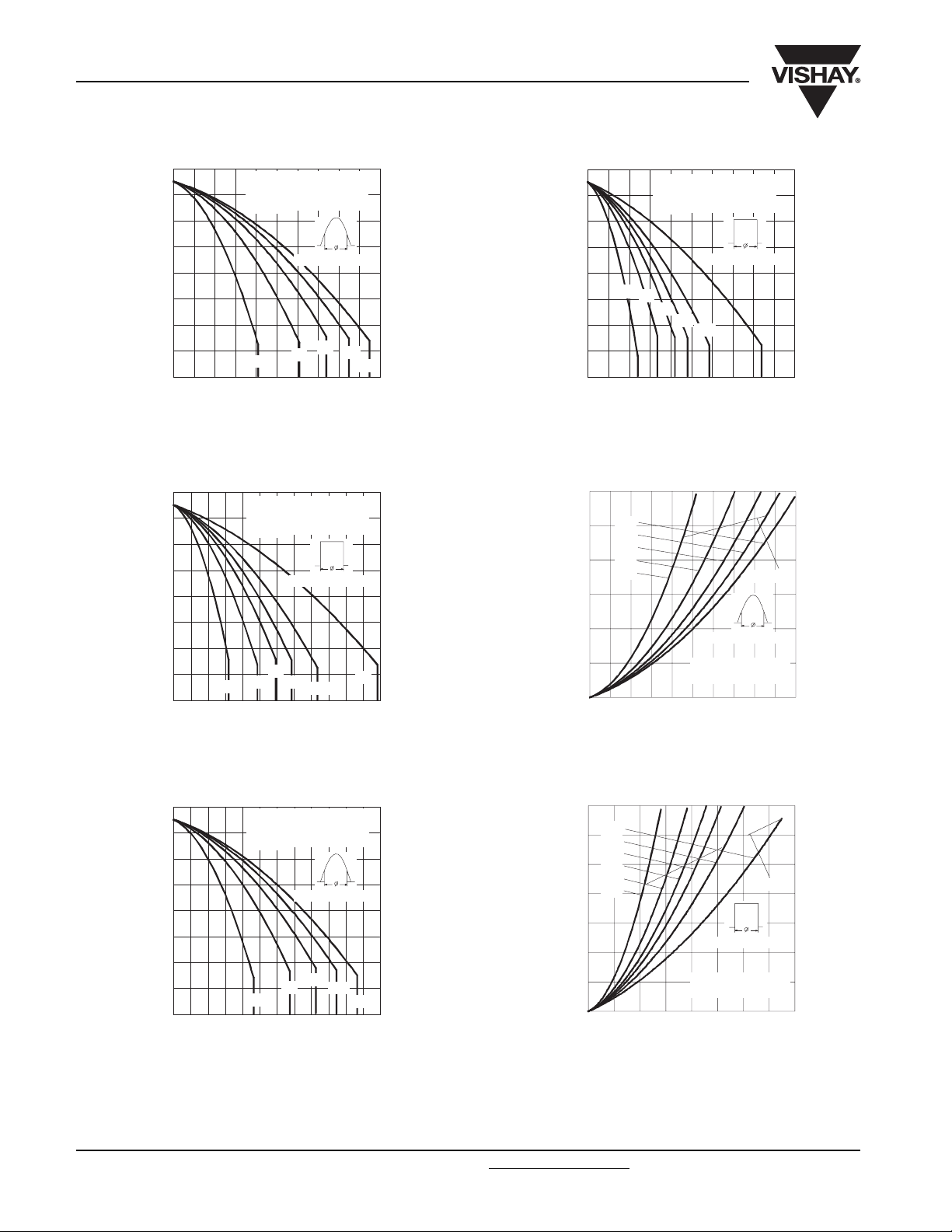
Fig. 5 - Current Ratings Characteristics
160
140
120
100
80
60
40
20
0
0 250 500 750 1000 1250 1500
Maximum Allowable Heatsink Temperature (°C)
Fig. 6 - Current Ratings Characteristics
SD 82 3C . . S20 C Se r i e s
(Double Side Cooled)
R (DC) = 0.038 K/ W
thJ-hs
Conduction Angle
90°
60°
30°
Average Forward Current (A)
SD 82 3C . . S2 0 C Se r i e s
(Double Side Cooled)
R (DC) = 0.038 K/W
thJ-hs
Cond uction Period
90°
60°
30°
Average Forward Current (A)
120°
180°
Fast Recovery Diodes
(Hockey PUK Version),
810/910 A
120°
180°
DC
160
140
120
100
80
60
40
20
0
0 400 800 1200 1600 2000
Maximum Allowable Heatsink Temperature (°C)
SD823C ..S30C Series
(Double Side Cooled)
R ( DC) = 0.038 K/W
thJ-hs
Conduction Period
30°
60°
90°
120°
180°
DC
Average Forward Current (A)
Fig. 8 - Current Ratings Characteristics
3000
2500
2000
1500
1000
500
Maximum Average Forwa rd Power Loss (W)
180°
120°
90°
60°
30°
SD 8 2 3C . . S20 C Se r i e s
T = 150°C
J
0
0 200 400 600 800 1000
Average Forward Current (A)
RM S Li m it
Cond uction Angle
Fig. 9 - Forward Power Loss Characteristics
160
140
120
100
80
60
40
20
0
0 200 400 600 800 1000 1200
Maximum Allowable Heatsink Temperature (°C)
SD823C ..S30C Series
(Doub le Side Cooled)
R (DC) = 0.038 K/ W
thJ-hs
Conduction Angle
90°
60°
30°
Average Forward Current (A)
Fig. 7 - Current Ratings Characteristics
120°
180°
3500
DC
3000
180°
120°
2500
90°
60°
30°
2000
1500
1000
500
0
Maximum Average Forward Power Loss (W)
0 200 400 600 800 1000 12001400 1600
Average Forward Current (A)
SD823C ..S20C Serie s
T = 1 50 °C
J
RM S Lim i t
Cond uction Period
Fig. 10 - Forward Power Loss Characteristics
www.vishay.com For technical questions, contact: ind-modules@vishay.com
Document Number: 93181
4 Revision: 14-May-08
Page 5

SD823C..C Series
3000
180°
120°
90°
60°
30°
SD823C ..S30C Serie s
T = 150°C
J
0 200 400 600 800 1000 1200
Average Forward Current (A)
RM S Li m i t
Cond uc tion Angle
Maximum Average Forward Power Loss (W)
2500
2000
1500
1000
500
0
Fig. 11 - Forward Power Loss Characteristics
3500
DC
3000
180°
120°
2500
90°
60°
30°
2000
1500
1000
500
0
Maximum Average Forward Power Loss (W)
0 400 800 1200 1600 2000
Av e ra ge Forw ard Curre n t (A)
SD 82 3C . . S30 C Se r i e s
T = 150°C
J
RM S Li m i t
Cond uction Period
Fig. 12 - Forward Power Loss Characteristics
Fast Recovery Diodes
(Hockey PUK Version),
810/910 A
Vishay High Power Products
10000
Peak Half Sine Wave Forward Current (A)
Fig. 14 - Maximum Non-Repetitive Surge Current
Peak Half Sine Wave Forward Current (A)
Fig. 15 - Maximum Non-Repetitive Surge Current
Maximum Non Re pe titive Surge Current
9000
8000
7000
6000
5000
4000
3000
SD 82 3C . . S20 C Se r ie s
2000
0.01 0.1 1
9000
At Any Rated Load Co ndition And With
Rated V Applied Following Surge.
8000
7000
6000
5000
4000
SD823C ..S30C Series
3000
110100
Number Of Equal Amplitude Half Cycle Current Pulses (N)
Versus Pulse Train Dura tion.
Pulse Tra in Dura t io n ( s)
RRM
Init ia l T = 150°C
No Voltage Reapplied
Rated V Reapplied
RRM
Init ia l T = 150 °C
@ 60 Hz 0.0083 s
@ 50 Hz 0.0100 s
J
J
9000
At Any Rated Load Condition And With
Rated V Applied Following Surge.
8000
7000
6000
5000
4000
3000
SD823C ..S20C Serie s
Peak Half Sine Wave Forward Current (A)
2000
110100
Numb er Of Equal Amplitude Half Cycle Current Pulses (N)
RRM
Initia l T = 150 °C
J
@ 60 Hz 0.0083 s
@ 50 Hz 0.0100 s
Fig. 13 - Maximum Non-Repetitive Surge Current
10000
Pea k Ha lf Sine Wave Fo rw a rd Cu rre n t (A)
Maximum Non Repetitive Surge Current
9000
8000
7000
6000
5000
4000
SD 82 3C . . S30 C Se r ie s
3000
2000
0.01 0.1 1
Versus Pulse Train Dura tion.
Pulse Train Duration (s)
Init ia l T = 150°C
No Vo lt a ge Rea p p li ed
Rated V Reapplied
RRM
J
Fig. 16 - Maximum Non-Repetitive Surge Current
Document Number: 93181 For technical questions, contact: ind-modules@vishay.com
www.vishay.com
Revision: 14-May-08 5
Page 6

SD823C..C Series
Vishay High Power Products
10000
T = 2 5 ° C
J
T = 150°C
J
1000
SD 8 2 3C . .S2 0 C Se r ie s
Instantaneous Forward Current (A)
100
0.5 1 1.5 2 2.5 3 3.5 4 4. 5 5
Instantaneous Forward Voltage (V)
Fig. 17 - Forward Voltage Drop Characteristics Fig. 18 - Forward Voltage Drop Characteristics
0.1
thJ-hs
SD 8 23 C . . S2 0 / S3 0C Se r ie s
Fast Recovery Diodes
(Hockey PUK Version),
810/910 A
Instantaneous Forward Current (A)
10000
T = 2 5 ° C
J
T = 150°C
1000
SD823C ..S30C Serie s
100
0.511.522.533.54
Instantaneous Forward Voltage (V)
J
0.01
0.001
Tran sient The rma l Impe danc e Z (K/W)
0.001 0.01 0.1 1 10 100
100
V
FP
80
60
40
Fo rw ard Rec overy (V)
20
0
0 400 800 1200 1600 2000
Rate Of Rise Of Forward Current - di/dt (A/us)
I
T = 150°C
J
T = 2 5 ° C
J
SD 8 2 3C . . S2 0 C Se ri e s
Sq uare Wave Pulse Duration (s)
Fig. 19 - Thermal Impedance Z
thJ-hs
Steady State Value
R = 0.076 K/ W
thJ-hs
(Single Side Cooled )
R = 0.038 K/ W
thJ-hs
(Double Side Co oled )
(DC Op eration)
Characteristic
100
V
FP
80
60
40
Fo rw a rd Re c o v e ry ( V)
20
0
0 400 800 1200 1600 2000
Rate Of Rise Of Forward Current - di/dt (A/us)
I
SD 82 3 C . . S3 0 C Se r i e s
T = 150°C
J
T = 2 5° C
J
Fig. 20 - Typical Forward Recovery Characteristics Fig. 21 - Typical Forward Recovery Characteristics
www.vishay.com For technical questions, contact: ind-modules@vishay.com
Document Number: 93181
6 Revision: 14-May-08
Page 7

SD823C..C Series
Fast Recovery Diodes
(Hockey PUK Version),
6
5.5
4.5
3.5
2.5
Maximum Reverse Recovery Time - Trr (µs)
Ra t e Of Fa l l O f Fo rw a r d Cu r re n t - d i / d t (A / µ s)
Fig. 22 - Recovery Time Characteristics
800
700
600
500
400
300
200
100
M a xi m um Re v e rse Re c o v e ry C ha rg e - Q rr ( µC )
Rate Of Fall Of Fo rward Current - di/d t (A/µs)
Fig. 23 - Recovery Charge Characteristics
SD823C ..S20C Se ries
T = 1 50 °C; V > 100V
J
5
4
3
2
10 100 1000
SD823C. .S20C Series
T = 150 °C ; V > 100V
J
0
0 50 100 150 200 250 300
I = 10 00 A
FM
Sin e Pulse
500 A
150 A
I = 10 00 A
FM
Si n e Pu l se
r
500 A
150 A
r
810/910 A
Vishay High Power Products
7
6.5
5.5
4.5
3.5
2.5
Maximum Reverse Recovery Time - Trr (µs)
Ra te O f Fa ll Of Forwa rd Cu rrent - di/ dt (A/µs)
Fig. 25 - Recovery Time Characteristics
1200
1000
800
600
400
200
M a x im u m Re v e r se Re c o v e r y C h a rg e - Q rr ( µC )
Rate Of Fall Of Forward Current - di/d t (A/ µs)
Fig. 26 - Recovery Charge Characteristics
SD 82 3 C . . S30 C Se ri e s
T = 150 °C ; V > 100V
6
5
4
3
2
0
J
10 100 1000
SD823C. .S30C Series
T = 150 °C ; V > 100V
J
0 50 100 150 200 250 300
r
I = 10 00 A
FM
Si n e Pu l se
500 A
150 A
I = 1000 A
FM
Si n e Pu l se
500 A
150 A
r
450
I = 1000 A
400
350
300
250
200
150
100
50
0
Ma xim um Re verse Rec ov ery Curren t - Irr (A)
0 50 100 150 200 250 300
Rate Of Fall Of Forward Current - di/dt (A/µs)
FM
Si n e Pu l se
500 A
150 A
SD 82 3C . . S2 0C Se r ie s
T = 150 °C ; V > 100V
J
r
Fig. 24 - Recovery Current Characteristics
550
500
450
400
350
300
250
200
150
100
50
0
Ma ximu m Reve rse Rec ov ery Cu rrent - Irr ( A)
0 50 100 150 200 250 300
Ra t e O f Fa l l O f Fo rw a r d C ur re n t - d i / d t (A / µ s)
I = 1000 A
FM
Si n e P u ls e
500 A
150 A
SD 82 3C . . S3 0C Se r i e s
T = 150 °C; V > 100V
J
r
Fig. 27 - Recovery Current Characteristics
Document Number: 93181 For technical questions, contact: ind-modules@vishay.com
www.vishay.com
Revision: 14-May-08 7
Page 8
SD823C..C Series
Vishay High Power Products
Fast Recovery Diodes
(Hockey PUK Version),
1E4
10 jo ules p er p ulse
6
4
2
1
0.6
1E3
Peak Forward Current (A)
1E2
1E1 1E2 1E3 1E4
Fig. 28 - Maximum Total Energy Loss Per Pulse Characteristics
1E4
3000
4000
6000
1E3
15000
Peak Forward Current (A)
20000
0.4
0.2
0.1
0.08
SD 82 3 C . . S20 C Se r i e s
Si n u so i d a l P u l se
T = 150°C, V = 800V
J
tp
d v/ dt = 1000V/ µs
Pulse Basewid th (µs)
2000
1000
400
10000
tp
RRM
200
100
50 Hz
SD 82 3 C . . S20 C Se r ie s
Si n u so i d a l P u l se
T = 55 ° C , V = 8 0 0V
C
dv/dt = 1000V/us
RRM
810/910 A
1E4
100
200
400
600
1000
2000
6000
10000
15000
4000
20000
3000
SD 82 3 C . . S20 C Se r i e s
Trapezoida l Pulse
T = 55°C, V = 800V
C
dv/dt = 1000V/us,
tp
di/ dt = 300A/us
RRM
1E3
Peak Forward Current (A)
1E2
1E1 1E2 1E3 1E4
Pulse Ba sew id t h ( µs)
Fig. 31 - Frequency Characteristics
1E4
SD 8 2 3C . . S2 0 C Se r i e s
Trap ezoidal Pulse
J
T = 15 0° C , V = 80 0 V
dv/dt = 1000V/µs
di/dt = 100A/µs
1E3
Peak Forward Current (A)
RRM
10 jo ules p er p ulse
6
4
2
1
0.6
0.4
0.2
50 Hz
tp
1E2
1E11E21E31E4
Pulse Ba se w id t h ( µs)
Fig. 29 - Frequency Characteristics
1E4
10 jo ul es pe r p ulse
6
4
2
1
1E3
Peak Forward Current (A)
tp
1E2
1 E1 1 E2 1 E3 1 E4
0.8
0.6
0.4
SD 82 3 C . . S20 C Se r i e s
Trapezoidal Pulse
T = 150°C , V = 800V
J
dv/dt = 1000V/µs
d i/d t = 300A/ µs
RRM
Pulse Basewidth (µs)
Fig. 30 - Maximum Total Energy Loss Per Pulse Characteristics
1E2
1E1 1E2 1E3 1E4
Pulse Ba sew id t h ( µs)
Fig. 32 - Maximum Total Energy Loss Per Pulse Characteristics
1E4
1000
600
2000
3000
10000
6000
4000
SD 82 3 C . . S20C Series
Tr a p e z o i d a l Pu l se
T = 55°C, V = 800V
C
dv/dt = 1000V/us,
tp
di/d t = 100A/us
1E3
Peak Forward Current (A)
1E2
15000
20000
1E1 1E2 1E3 1E4
50 Hz100
200400
RRM
Pulse Ba se wi dt h (µs)
Fig. 33 - Frequency Characteristics
www.vishay.com For technical questions, contact: ind-modules@vishay.com
Document Number: 93181
8 Revision: 14-May-08
Page 9

SD823C..C Series
Fast Recovery Diodes
(Hockey PUK Version),
810/910 A
1E4
10 jo ule s p er p ulse
6
4
2
1
0.6
0.4
1E3
Pe ak Forwa rd Curren t (A)
1E2
1E1 1E2 1E3 1E4
Fig. 34 - Maximum Total Energy Loss Per Pulse Characteristics
1E4
1E3
Peak Forward Current (A)
20000
1E2
1E1 1E2 1E3 1E4
Fig. 35 - Frequency Characteristics
0.2
0.1
SD82 3C..S30C Series
Si n u so i d a l Pu l s e
T = 150°C, V = 800V
J
tp
d v/d t = 1000V/ µs
Pulse Ba se wi dt h (µ s)
2000
3000
4000
6000
10000
15000
Pu lse Ba se wid t h ( µs)
RRM
1000
400
SD 8 23 C . . S3 0C Se r i e s
Sinusoida l Pulse
T = 55°C, V = 800V
C
tp
dv/dt = 1000V/us
200
50 Hz
100
RRM
Vishay High Power Products
1E4
50 Hz
100
200
400
600
1000
1500
1E3
Pea k Forw a rd C urre nt (A)
1E2
1E1 1E2 1E3 1E4
1E4
1E3
Peak Forward Current (A)
1E2
1E1 1E2 1E3 1E4
Fig. 38 - Maximum Total Energy Loss Per Pulse Characteristics
2000
3000
4000
6000
10000
15000
SD 82 3 C . .S3 0 C Se r ie s
Trap ezoida l Pulse
T = 55°C, V = 800V
C
dv/dt = 1000V/us,
tp
di/dt = 300A/us
Pu lse Ba se w id t h (µ s)
Fig. 37 - Frequency Characteristics
10 jo ule s p er p ulse
6
4
2
1
0.6
0.4
SD 8 23 C . . S30 C Se r i e s
Trapezoidal Pulse
T = 150°C, V = 800V
J
dv/dt = 1000V/µs
tp
di/dt = 100A/µs
RRM
Pu lse Ba se wid t h ( µs)
RRM
1E4
10 jo ule s p er p ulse
6
4
2
1E3
Peak Forward Current (A)
0.4
1E2
tp
1E11E21E31E4
1
0.8
0.6
SD82 3C..S30C Serie s
Trap ezoida l Pulse
T = 1 5 0 ° C , V = 8 0 0 V
J
dv/dt = 1000V/µs
di/dt = 300A/µs
RRM
Pulse Basewidth (µs)
Fig. 36 - Maximum Total Energy Loss Per Pulse Characteristics
1E4
400
200
3000
2000
6000
1000
4000
100
1E3
10000
SD 8 23 C . . S3 0C Se r i e s
Peak Forward Current (A)
1E2
1E1 1E2 1E3 1E4
15000
20000
Sinusoida l Pulse
T = 55°C, V = 800V
C
tp
dv/dt = 1000V/us
RRM
Pu lse Ba se wid t h ( µs)
Fig. 39 - Frequency Characteristics
50 Hz
Document Number: 93181 For technical questions, contact: ind-modules@vishay.com
www.vishay.com
Revision: 14-May-08 9
Page 10
SD823C..C Series
Vishay High Power Products
ORDERING INFORMATION TABLE
Device code
SD 82 3 C 25 S20 C
1 - Diode
2 - Essential part number
3 - 3 = Fast recovery
4 - C = Ceramic PUK
5 - Voltage code x 100 = V
6 -t
7 - C = PUK case B-43
Fast Recovery Diodes
(Hockey PUK Version),
810/910 A
51324
(see Voltage Ratings table)
RRM
code
rr
67
www.vishay.com For technical questions, contact: ind-modules@vishay.com
10 Revision: 14-May-08
Document Number: 93181
Page 11

DIMENSIONS in millimeters (inches)
3.5 (0.14) DIA. NOM. x
1.8 (0.07) deep MIN. both ends
Outline Dimensions
Vishay High Power Products
B-43
42 (1.65) DIA. MAX.
0.8 (0.03) MIN.
both ends
14.4 (0.57)
15.4 (0.61)
Quote between upper and lower pole pieces has to be considered after
application of mounting force (see Thermal and Mechanical Specifications)
25.3 (1) DIA. MAX.
2 places
40.5 (1.59) DIA. MAX.
Document Number: 95249 For technical questions concerning discrete products, contact: diodes-tech@vishay.com
Revision: 26-Nov-07 For technical questions concerning module products, contact: ind-modules@vishay.com
www.vishay.com
1
Page 12

Legal Disclaimer Notice
Vishay
Notice
The products described herein were acquired by Vishay Intertechnology, Inc., as part of its acquisition of
International Rectifier’s Power Control Systems (PCS) business, which closed in April 2007. Specifications of the
products displayed herein are pending review by Vishay and are subject to the terms and conditions shown below.
Specifications of the products displayed herein are subject to change without notice. Vishay Intertechnology, Inc., or
anyone on its behalf, assumes no responsibility or liability for any errors or inaccuracies.
Information contained herein is intended to provide a product description only. No license, express or implied, by
estoppel or otherwise, to any intellectual property rights is granted by this document. Except as provided in Vishay's
terms and conditions of sale for such products, Vishay assumes no liability whatsoever, and disclaims any express
or implied warranty, relating to sale and/or use of Vishay products including liability or warranties relating to fitness
for a particular purpose, merchantability, or infringement of any patent, copyright, or other intellectual property right.
The products shown herein are not designed for use in medical, life-saving, or life-sustaining applications.
Customers using or selling these products for use in such applications do so at their own risk and agree to fully
indemnify Vishay for any damages resulting from such improper use or sale.
®
International Rectifier
are registered trademarks of International Rectifier Corporation in the U.S. and other countries. All other product
names noted herein may be trademarks of their respective owners.
, IR®, the IR logo, HEXFET®, HEXSense®, HEXDIP®, DOL®, INTERO®, and POWIRTRAIN
®
Document Number: 99901 www.vishay.com
Revision: 12-Mar-07 1
 Loading...