

Page 1
DO-200AB (B-PUK)
PRODUCT SUMMARY
I
F(AV)
Vishay High Power Products
Standard Recovery Diodes
(Hockey PUK Version), 1200 A
FEATURES
• Wide current range
• High voltage ratings up to 4500 V
• High surge current capabilities
• Diffused junction
• Hockey PUK version
• Case style DO-200AB (B-PUK)
• Lead (Pb)-free
TYPICAL APPLICATIONS
• Converters
• Power supplies
1200 A
• Machine tool controls
• High power drives
• Medium traction applications
SD800C..L Series
RoHS
COMPLIANT
MAJOR RATINGS AND CHARACTERISTICS
PARAMETER TEST CONDITIONS
I
F(AV)
I
F(RMS)
I
FSM
2
I
t
V
RRM
T
J
T
hs
T
hs
50 Hz 13 600 12 200
60 Hz 14 240 12 800
50 Hz 925 745
60 Hz 845 680
Range 2400 to 3600 4000 to 4500 V
ELECTRICAL SPECIFICATIONS
VOLTAGE RATINGS
V
, MAXIMUM REPETITIVE
TYPE NUMBER
SD800C..L
VOLTAGE
CODE
24 2400 2500
30 3000 3100
36 3600 3700
40 4000 4100
45 4500 4600
RRM
PEAK REVERSE VOLTAGE
V
SD800C..L
24 TO 36 40 TO 45
1180 1065 A
55 55 °C
2280 2040 A
25 25 °C
- 40 to 150 - 40 to 150 °C
V
, MAXIMUM NON-REPETITIVE
RSM
PEAK REVERSE VOLTAGE
V
AT T
I
RRM
UNITS
A
kA2s
MAXIMUM
= TJ MAXIMUM
J
mA
50
Page 2
SD800C..L Series
Vishay High Power Products
Standard Recovery Diodes
(Hockey PUK Version),
1200 A
FORWARD CONDUCTION
PARAMETER SYMBOL TEST CONDITIONS
Maximum average forward current
at heatsink temperature
Maximum RMS forward current I
Maximum peak, one-cycle forward,
non-repetitive surge current
Maximum I
Maximum I
2
t for fusing I2t
2
√t for fusing I2√t t = 0.1 to 10 ms, no voltage reapplied 9250 7450 kA2√s
Low level value of threshold voltage V
High level value of threshold voltage V
Low level value of forward
slope resistance
High level value of forward
slope resistance
Maximum forward voltage drop V
I
F(AV)
F(RMS)
I
FSM
F(TO)1
F(TO)2
r
r
180° conduction, half sine wave
Double side (single side) cooled
25 °C heatsink temperature double side cooled 2280 2040
t = 10 ms
t = 8.3 ms 14 240 12 800
t = 10 ms
t = 8.3 ms 11 980 10 750
t = 10 ms
t = 8.3 ms 845 680
t = 10 ms
t = 8.3 ms 597 480
(16.7 % x π x I
(I > π x I
(16.7 % x π x I
f1
(I > π x I
f2
Ipk = 2000 A, TJ = TJ maximum,
FM
t
= 10 ms sinusoidal wave
p
No voltage
reapplied
50 % V
RRM
reapplied
No voltage
reapplied
50 % V
RRM
reapplied
< I < π x I
F(AV)
), TJ = TJ maximum 1.10 1.18
F(AV)
< I < π x I
F(AV)
), TJ = TJ maximum 0.34 0.41
F(AV)
F(AV)
F(AV)
SD800C..L
24 TO 36 40 TO 45
1180 (550) 1065 (490) A
55 (85) 55 (85) °C
13 600 12 200
11 440 10 250
Sinusoidal half wave,
initial T
= TJ maximum
J
925 745
654 526
), TJ = TJ maximum 0.90 1.06
), TJ = TJ maximum 0.38 0.44
1.66 1.95 V
UNITS
A
2
kA
V
mΩ
s
THERMAL AND MECHANICAL SPECIFICATIONS
PARAMETER SYMBOL TEST CONDITIONS VALUES UNITS
Maximum junction operating
temperature range
Maximum storage temperature range T
Maximum thermal resistance,
junction to heatsink
Mounting force, ± 10 % 14 700 (1500) N (kg)
Approximate weight 255 g
Case style See dimensions - link at the end of datasheet DO-200AB (B-PUK)
ΔR
CONDUCTION ANGLE
CONDUCTION
thJ-hs
SINUSOIDAL CONDUCTION RECTANGULAR CONDUCTION
SINGLE SIDE DOUBLE SIDE SINGLE SIDE DOUBLE SIDE
180° 0.009 0.009 0.006 0.006
120° 0.011 0.011 0.011 0.011
90° 0.014 0.014 0.015 0.015
60° 0.020 0.020 0.021 0.021
30° 0.036 0.036 0.036 0.036
Note
• The table above shows the increment of thermal resistance R
R
T
J
Stg
thJ-hs
- 40 to 150
- 55 to 200
DC operation single side cooled 0.073
DC operation double side cooled 0.031
TEST CONDITIONS UNITS
= TJ maximum K/W
T
J
when devices operate at different conduction angles than DC
thJ-hs
°C
K/W
Page 3
SD800C..L Series
150
140
130
120
110
100
90
80
70
60
50
40
30
Maximum Allowable Heatsink Temperature (°C)
SD800C. .L Series (2400V to 3600V )
0 100 200 300 40 0 5 0 0 60 0 700 800 900
Avera ge Forw ard Current (A )
(Single Side Cooled)
R (DC) = 0.073 K/W
thJ-h s
Conduction Angle
30°
60°
90°
120°
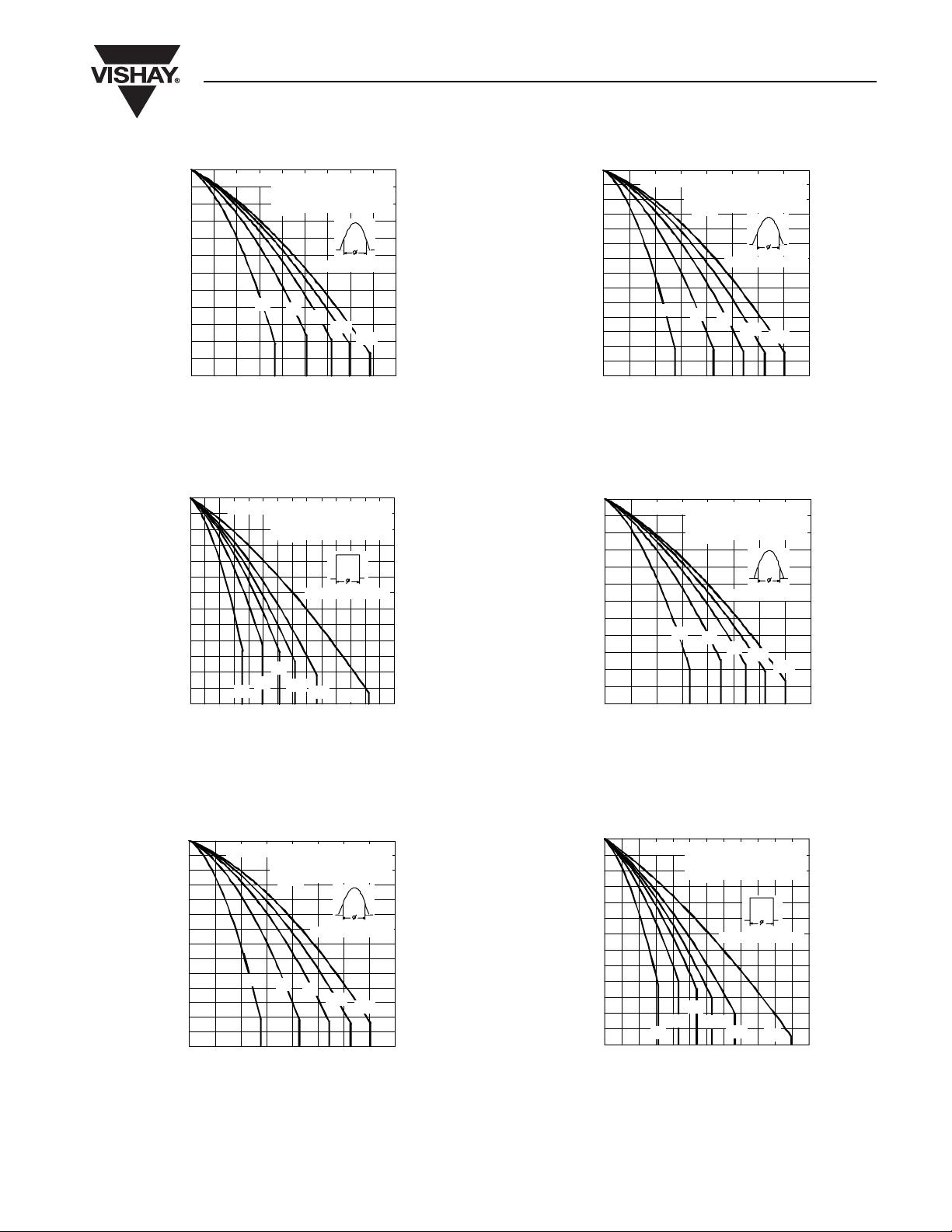
Fig. 1 - Current Ratings Characteristics
150
140
130
120
110
100
90
80
70
60
50
40
30
20
Maximum Allowable Heatsink Tem perature (°C)
SD 800C ..L Series (2400V to 3600 V )
30°
0 200 400 600 800 1000 1200 1400
Average Forward Current (A)
( S in g l e S i d e C oo le d )
R ( D C ) = 0 .0 73 K / W
th J-hs
Conduction Period
90°
60°
120°
180°
Fig. 2 - Current Ratings Characteristics
Standard Recovery Diodes
(Hockey PUK Version),
1200 A
180°
DC
Vishay High Power Products
150
140
130
120
110
100
90
80
70
60
50
40
30
20
10
Maximum Allowable Heatsink Temperature (°C)
150
140
130
120
110
100
90
80
70
60
50
40
30
Maximum Allowable Heatsink Temperature ( °C)
SD800C..L Series (2400V to 36 00V )
0 400 800 1200 1600
Avera ge Forwa rd Curren t (A )
(Double S ide Cooled)
R (DC) = 0.031 K/W
th J-hs
Cond uction Angle
30°
60°
90°
120°
180°
Fig. 4 - Current Ratings Characteristics
SD800C. .L Series (4000V to 450 0V )
0 100 20 0 3 0 0 4 0 0 5 00 600 70 0 8 0 0
Average Forward Current (A)
(Single Side Co oled )
R (DC ) = 0 . 07 3 K/ W
thJ-h s
Conduction Angle
30°
60°
90°
120°
180°
Fig. 5 - Current Ratings Characteristics
150
140
130
120
110
100
90
80
70
60
50
40
30
20
10
Maximum Allowable Heatsink Temperature (°C)
SD800C..L Series (2400V to 36 00V )
0 400 800 1200 1600
Avera ge Forwa rd Curren t (A )
(Double S ide Cooled)
R (DC) = 0.031 K/W
th J-hs
Cond uction Angle
30°
60°
90°
120°
Fig. 3 - Current Ratings Characteristics
180°
150
140
130
120
110
100
90
80
70
60
50
40
30
20
M axim um Allow able Heatsin k Tem pera ture (°C)
SD 800C ..L Se rie s (4 000V to 4500V )
30°
0 2 00 4 00 6 00 80 0 1 00 0 1200
Average Forw ard Current (A)
( S in g l e S i d e C oo le d )
R (D C ) = 0.073 K /W
thJ-h s
Conduction Period
90°
60°
120°
180°
Fig. 6 - Current Ratings Characteristics
DC
Page 4

SD800C..L Series
Vishay High Power Products
150
140
130
120
110
100
90
80
70
60
50
40
30
20
Maximum Allowable Heatsink Tem perature (°C)
150
140
130
120
110
100
90
80
70
60
50
40
30
20
Maximum Allow able Heatsin k Temperature (°C)
SD800C. .L Series (4000V to 4500V )
0 200 400 600 800 1000 1200 1400
Averag e F orw ard C ur re nt (A)
(Double Side Cooled)
R (DC ) = 0 .03 1 K /W
thJ-h s
Con duc tion A ngle
30°
60°
90°
120°
Fig. 7 - Current Ratings Characteristics
SD 80 0C ..L Serie s (4000V to 4500V )
30°
60°
0 400 80 0 12 0 0 1 60 0 200 0 240 0
Average Forw ard C urrent (A)
(Dou ble Sid e C ooled)
R ( D C ) = 0.031 K/W
thJ-h s
Conduction Period
90°
120°
180°
DC
Fig. 8 - Current Ratings Characteristics
Standard Recovery Diodes
(Hockey PUK Version),
1200 A
180°
4500
4000
DC
180°
3500
120°
90°
3000
60°
30°
2500
2000
1500
1000
500
0
Maximum Average Forward Power Loss (W)
0 500 1000 1500 2000 2500
Average Forward Current (A)
RMS Limit
Conduction Period
SD800C..L Series
(2400V to 3600 V)
T = 150°C
J
Fig. 10 - Forward Power Loss Characteristics
3500
3000
2500
2000
1500
1000
500
Maximum Average Forward Power Loss (W)
180°
120°
90°
60°
30°
0
0 20 0 400 6 00 80 0 1 00 0 120 0 14 0 0
Average Forward Current (A)
RMS Limit
Conduction Angle
SD800C..L Series
(4000V to 4500V )
T = 150°C
J
Fig. 11 - Forward Power Loss Characteristics
3500
3000
2500
2000
1500
1000
500
M aximum Averag e Forwar d Pow er Loss ( W)
180°
120°
90°
60°
30°
0
0 200 40 0 6 0 0 80 0 10 0 0 120 0 140 0 160 0
Average Forward Current (A)
RMS Limit
Conduction Angle
SD800C..L Series
(2400V to 3600V )
T = 150°C
J
Fig. 9 - Forward Power Loss Characteristics
4500
4000
3500
3000
2500
2000
1500
1000
Maximum Average Forward Power Loss (W)
DC
180°
120°
90°
60°
30°
500
0
0 400 800 1200160020002400
Average Forward Current (A)
RMS Limit
Conduction Period
SD8 00C..L S er ies
(4000V to 45 00V )
T = 150°C
J
Fig. 12 - Forward Power Loss Characteristics
Page 5

SD800C..L Series
Standard Recovery Diodes
(Hockey PUK Version),
14000
At An y Rated Load C ond ition An d W ith
50% Rated V Applied Following Surge
13000
12000
11000
10000
9000
8000
7000
6000
5000
SD 8 00C ..L Se rie s
(2400V to 3600V )
4000
Peak Half Sine W ave Forw ard Current (A)
3000
Number Of Equal Am plitude Half Cycle Current Pulses (N)
Fig. 13 - Maximum Non-Repetitive Surge Current
Single and Double Side Cooled
15000
Maximum Non Repetitive Surge Current
14000
13000
12000
11000
10000
9000
8000
7000
6000
5000
SD800C..L Series
(2400V to 360 0V)
4000
Pea k Half Sine W ave Fo rward C urren t (A)
3000
Fig. 14 - Maximum Non-Repetitive Surge Current
Single and Double Side Cooled
RRM
Versus Pulse Train Duration.
50% Rated V Reapplied
Pulse Train Duration (s)
In it i a l T = 1 5 0° C
@ 60 H z 0.0083 s
@ 50 H z 0.0100 s
In it ia l T = 15 0 °C
No Voltage Reapplied
RRM
J
001011
J
11.010.0
1200 A
Vishay High Power Products
14000
M a xim u m No n R ep e t itive Surg e C u rre n t
12000
10000
8000
6000
4000
SD 8 00C ..L Se rie s
Pe ak H a lf Sine W a ve Forw ar d C u rre n t ( A)
(4000V to 45 00V )
2000
0.01 0.1 1
Fig. 16 - Maximum Non-Repetitive Surge Current
Single and Double Side Cooled
100 0 0
100 0
Instantaneous Forward Current (A)
100
0.5 1 1.5 2 2. 5 3 3.5 4 4.5
Instantaneous Forward Voltage (V)
Fig. 17 - Forward Voltage Drop Characteristics
Ve rsu s P u lse T rain D ura tion.
N o V o lta g e R e a p p l ie d
50 % R a ted V Re a p p lied
Pulse Train Duration (s)
T = 25°C
J
SD800C..L Series
(2400V to 360 0V)
Initia l T = 15 0 °C
J
RRM
T = 150°C
J
120 0 0
At Any Rated L oad Condition And With
50 % Rate d V A p p l ie d F o ll o w in g Surg e
110 0 0
100 0 0
9000
8000
7000
6000
5000
SD800C..L Series
4000
Peak Half Sine Wave Forward Current (A)
(4000V to 4500V )
3000
Number Of E qua l Am plitude Half Cycle C urrent Pulses (N)
RRM
Initial T = 150°C
J
@ 60 Hz 0.0083 s
@ 50 Hz 0.0100 s
Fig. 15 - Maximum Non-Repetitive Surge Current
Single and Double Side Cooled
10000
T = 25° C
J
T = 150°C
J
1000
SD 8 00C ..L Se rie s
Instantaneous Forward Current (A)
100
001011
0.5 1 1.5 2 2.5 3 3.5 4 4.5 5 5.5
Instantaneous Forw ard Voltage (V)
(4000V to 4500V )
Fig. 18 - Forward Voltage Drop Characteristics
Page 6

SD800C..L Series
Vishay High Power Products
0.1
Stea d y St a te Va lue
R = 0.073 K/W
thJ-h s
(Single Sid e C oo led)
R = 0.031 K/W
thJ-h s
T ransien t The rm a l Im pe d anc e Z (K/W )
ORDERING INFORMATION TABLE
Device code
thJ-hs
(Dou ble Side Cooled)
(D C O p era tion)
0.01
0.001
0.001 0.01 0.1 1 10 100
Fig. 19 - Thermal Impedance Z
SD 80 0 C 45 L
Standard Recovery Diodes
(Hockey PUK Version),
1200 A
SD 80 0C ..L Serie s
Sq uar e W a ve Pulse D uration (s)
Characteristics
thJ-hs
1 - Diode
2 - Essential part number
3 - 0 = Standard recovery
4 - C = Ceramic PUK
5 - Voltage code x 100 = V
6 -
L = PUK case DO-200AB (B-PUK)
51324
6
(see Voltage Ratings table)
RRM
Page 7

DIMENSIONS in millimeters (inches)
3.5 (0.14) DIA. NOM. x
1.8 (0.07) deep MIN. both ends
Outline Dimensions
Vishay High Power Products
DO-200AB (B-PUK)
58.5 (2.30) DIA. MAX.
0.8 (0.03)
both ends
25.4 (1)
26.9 (1.06)
Quote between upper and lower pole pieces has to be considered after
application of mounting force (see Thermal and Mechanical Specifications)
34 (1.34) DIA. MAX.
2 places
53 (2.09) DIA. MAX.
Document Number: 95246 For technical questions concerning discrete products, contact: diodes-tech@vishay.com
Revision: 05-Nov-07 For technical questions concerning module products, contact: ind-modules@vishay.com
www.vishay.com
1
Page 8

Legal Disclaimer Notice
Vishay
Disclaimer
All product specifications and data are subject to change without notice.
Vishay Intertechnology, Inc., its affiliates, agents, and employees, and all persons acting on its or their behalf
(collectively, “Vishay”), disclaim any and all liability for any errors, inaccuracies or incompleteness contained herein
or in any other disclosure relating to any product.
Vishay disclaims any and all liability arising out of the use or application of any product described herein or of any
information provided herein to the maximum extent permitted by law. The product specifications do not expand or
otherwise modify Vishay’s terms and conditions of purchase, including but not limited to the warranty expressed
therein, which apply to these products.
No license, express or implied, by estoppel or otherwise, to any intellectual property rights is granted by this
document or by any conduct of Vishay.
The products shown herein are not designed for use in medical, life-saving, or life-sustaining applications unless
otherwise expressly indicated. Customers using or selling Vishay products not expressly indicated for use in such
applications do so entirely at their own risk and agree to fully indemnify Vishay for any damages arising or resulting
from such use or sale. Please contact authorized Vishay personnel to obtain written terms and conditions regarding
products designed for such applications.
Product names and markings noted herein may be trademarks of their respective owners.
Document Number: 91000 www.vishay.com
Revision: 18-Jul-08 1
 Loading...