

Page 1
Vishay High Power Products
Standard Recovery Diodes
(Hockey PUK Version), 700 A
FEATURES
• Wide current range
SD700C..L Series
• High voltage ratings up to 4500 V
• High surge current capabilities
• Diffused junction
• Hockey PUK version
DO-200AB (B-PUK)
• Case style DO-200AB (B-PUK)
• Lead (Pb)-free
TYPICAL APPLICATIONS
PRODUCT SUMMARY
I
F(AV)
700 A
• Converters
• Power supplies
• High power drives
• Auxiliary system supplies for traction applications
MAJOR RATINGS AND CHARACTERISTICS
PARAMETER TEST CONDITIONS VALUES UNITS
I
F(AV)
I
F(RMS)
I
FSM
2
I
t
V
RRM
T
J
T
hs
T
hs
50 Hz 7500
60 Hz 7850
50 Hz 281
60 Hz 257
Range 3000 to 4500 V
700 A
55 °C
1310 A
25 °C
A
kA2s
- 40 to 150 °C
RoHS
COMPLIANT
ELECTRICAL SPECIFICATIONS
VOLTAGE RATINGS
V
TYPE NUMBER
SD700C..L
VOLTAGE
CODE
30 3000 3100
36 3600 3700
40 4000 4100
45 4600 4600
RRM
PEAK REVERSE VOLTAGE
, MAXIMUM REPETITIVE
V
V
, MAXIMUM NON-REPETITIVE
RSM
PEAK REVERSE VOLTAGE
V
I
MAXIMUM
RRM
AT T
= TJ MAXIMUM
J
mA
50
Page 2
SD700C..L Series
Vishay High Power Products
Standard Recovery Diodes
(Hockey PUK Version), 700 A
FORWARD CONDUCTION
PARAMETER SYMBOL TEST CONDITIONS VALUES UNITS
Maximum average forward current
at heatsink temperature
Maximum RMS forward current I
Maximum peak, one-cycle forward,
non-repetitive surge current
Maximum I
Maximum I
2
t for fusing I2t
2
√t for fusing I2√t t = 0.1 to 10 ms, no voltage reapplied 2810 kA2√s
Low level value of threshold voltage V
High level value of threshold voltage V
Low level value of forward
slope resistance
High level value of forward
slope resistance
Maximum forward voltage drop V
I
F(AV)
F(RMS)
I
FSM
F(TO)1
F(TO)2
r
f1
r
f2
FM
180° conduction, half sine wave
Double side (single side) cooled
25 °C heatsink temperature double side cooled 1310
t = 10 ms
t = 8.3 ms 7850
t = 10 ms
t = 8.3 ms 6600
t = 10 ms
t = 8.3 ms 257
t = 10 ms
t = 8.3 ms 182
(16.7 % x π x I
(I > π x I
(16.7 % x π x I
(I > π x I
No voltage
reapplied
100 % V
reapplied
No voltage
RRM
Sinusoidal half wave,
initial T
= TJ maximum
J
reapplied
100 % V
RRM
reapplied
< I < π x I
F(AV)
), TJ = TJ maximum 0.99
F(AV)
< I < π x I
F(AV)
), TJ = TJ maximum 0.73
F(AV)
), TJ = TJ maximum 0.88
F(AV)
), TJ = TJ maximum 0.78
F(AV)
Ipk = 1000 A, TJ = TJ maximum, tp = 10 ms sinusoidal wave 1.66 V
700 (345) A
55 (85) °C
7500
6310
281
199
A
kA2s
V
mΩ
THERMAL AND MECHANICAL SPECIFICATIONS
PARAMETER SYMBOL TEST CONDITIONS VALUES UNITS
Maximum junction operating
temperature range
Maximum storage temperature range T
Maximum thermal resistance,
junction to heatsink
Mounting force, ± 10 %
Approximate weight 250 g
Case style See dimensions - link at the end of datasheet DO-200AB (B-PUK)
ΔR
CONDUCTION ANGLE
CONDUCTION
thJ-hs
SINUSOIDAL CONDUCTION RECTANGULAR CONDUCTION
SINGLE SIDE DOUBLE SIDE SINGLE SIDE DOUBLE SIDE
180° 0.011 0.011 0.008 0.008
120° 0.014 0.015 0.014 0.014
90° 0.018 0.018 0.019 0.019
60° 0.026 0.026 0.027 0.028
30° 0.045 0.046 0.046 0.046
Note
• The table above shows the increment of thermal resistance R
R
T
J
Stg
thJ-hs
- 40 to 150
- 55 to 200
DC operation single side cooled 0.011
DC operation double side cooled 0.05
9800
(1000)
TEST CONDITIONS UNITS
= TJ maximum K/W
T
J
when devices operate at different conduction angles than DC
thJ-hs
°C
K/W
N
(kg)
Page 3
SD700C..L Series
Standard Recovery Diodes
(Hockey PUK Version), 700 A
150
140
130
120
110
100
90
80
70
60
50
40
30
0 100 200 300 400 500
Maximum Allowable Heatsink Temperature (°C)
Average Forward Current (A)
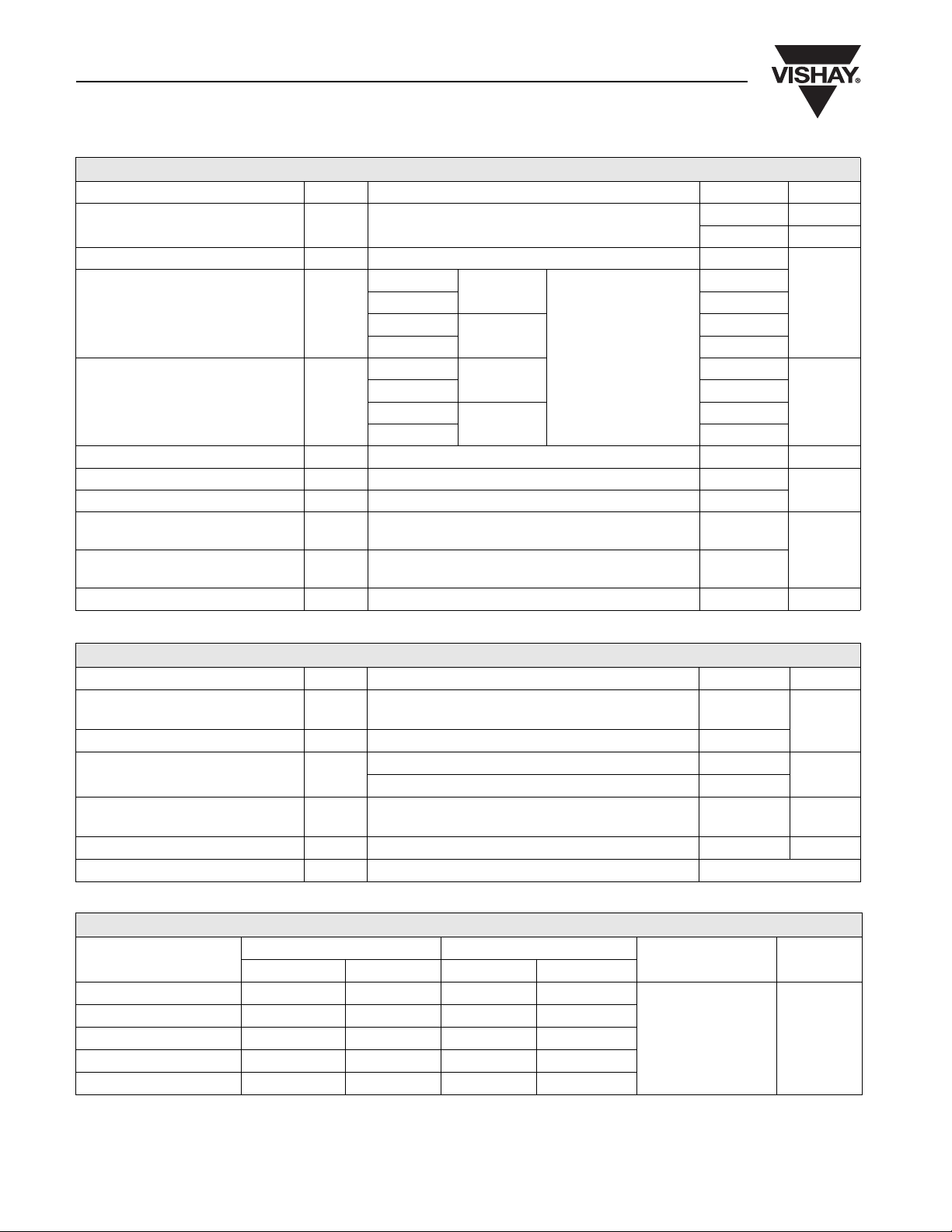
Fig. 1 - Current Ratings Characteristics
150
140
130
120
110
100
90
80
70
60
50
40
30
20
0200400600800
Maximum Allowable Heatsin k Temperature (°C)
Average Forward Current (A)
Fig. 2 - Current Ratings Characteristics
SD700C ..L Series
(Single Side Cooled)
R (DC ) = 0. 11 K/ W
th J-hs
30°
60°
SD700C ..L Series
(Single Side Cooled)
R (D C) = 0.11 K/W
th J-hs
30°
60°
90°
120°
Conduction Angle
90°
120°
180°
Conduction Period
180°
DC
Vishay High Power Products
150
140
130
120
110
100
90
80
70
60
50
40
30
20
0 200 400 600 800 1000 1200 1400
Maximum Allowable Heatsink Temperature (°C)
Fig. 4 - Current Ratings Characteristics
2500
2000
1500
1000
500
0
Maximum Average Forward Power Loss (W)
0 200 400 600 800 1000
Fig. 5 - Forward Power Loss Characteristics
SD700C..L Series
(Double Side Cooled)
R (DC) = 0.05 K/W
thJ- hs
Con duction Period
30°
60°
90°
120°
180°
Average Forward Current (A)
180°
120°
90°
60°
30°
Con duction An gle
SD700C..L Series
T = 150°C
J
Average Forward Current (A)
DC
RMS Lim it
180
160
140
120
100
80
60
40
20
0
0 5 0 0 100 0 150 0 200 0 2500
Maximum Allowable Heatsink Temperature ( °C)
SD2000C..L Series
(Double Side Cooled)
R (DC ) = 0. 03 1 K/W
th J-hs
Conduction Angle
30°
60°
90°
Ave rage F orward Current (A)
Fig. 3 - Current Ratings Characteristics
120°
180°
2500
DC
180°
2000
120°
90°
60°
1500
30°
1000
500
0
Maximum Average Forw ard Power Loss (W)
0 200 400 600 800 1000 1200 1400
Aver a ge Fo rw ard Curre nt (A)
RMS Lim it
Conduction Period
SD 700C.. L Ser ies
T = 150°C
J
Fig. 6 - Forward Power Loss Characteristics
Page 4
SD700C..L Series
Vishay High Power Products
700 0
At Any Rated Load Condition And With
50% Rated V Applied Fo llowin g Surge
600 0
500 0
400 0
300 0
SD700C ..L Series
Peak Half Sine Wave Forward Current (A)
200 0
N u m be r O f E q ua l A m p lit ud e H alf C yc le C u rre nt P uls es (N )
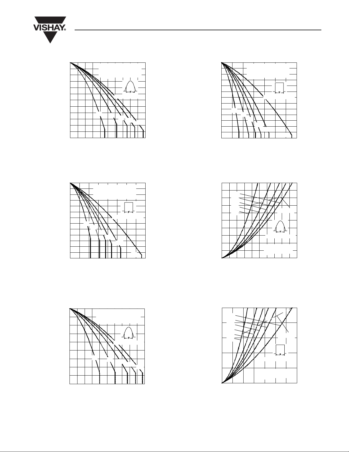
Fig. 7 - Maximum Non-Repetitive Surge Current
Single and Double Side Cooled
RRM
Initial T = 150 °C
J
@ 60 Hz 0.0083 s
@ 50 Hz 0.0100 s
Standard Recovery Diodes
(Hockey PUK Version), 700 A
9000
8000
7000
6000
5000
4000
3000
2000
Peak Half Sine Wave Forward Current (A)
1000
001011
10000
0.01 0.1 1
Fig. 8 - Maximum Non-Repetitive Surge Current
Maximum Non Repetitive Surge Current
SD7 00C ..L S eri es
Versus Pulse Train Duration.
50% Rated V Reapplied
Pulse Train Duration (s)
In itial T = 15 0 °C
No Voltage Reapplied
RRM
J
Single and Double Side Cooled
thJ-hs
1
0.1
0.01
100 0
Instant an eous Forward C urrent (A)
100
0.511.522.533.54
Fig. 9 - Forward Voltage Drop Characteristics
Steady State Value
R = 0.11 K/W
thJ-h s
(Single Side Cooled )
R = 0.05 K/W
thJ-h s
(Double Side Cooled)
(D C O pe ration )
T = 25°C
J
T = 150°C
J
SD 700C ..L Series
Instantaneous Forward Voltage (V)
SD700C..L Series
Transient Therma l Imp eda nce Z (K/W )
0.001
Square W ave Pulse Duratio n (s)
Fig. 10 - Thermal Impedance Z
Characteristics
thJ-hs
0111.010.0100.0
Page 5

SD700C..L Series
Standard Recovery Diodes
(Hockey PUK Version), 700 A
ORDERING INFORMATION TABLE
Device code
SD 70 0 C 45 L
1 - Diode
2 - Essential part number
3 - 0 = Standard recovery
4 - C = Ceramic PUK
5 - Voltage code x 100 = V
6 -
Vishay High Power Products
51324
L = PUK case DO-200AB (B-PUK)
6
(see Voltage Ratings table)
RRM
Page 6
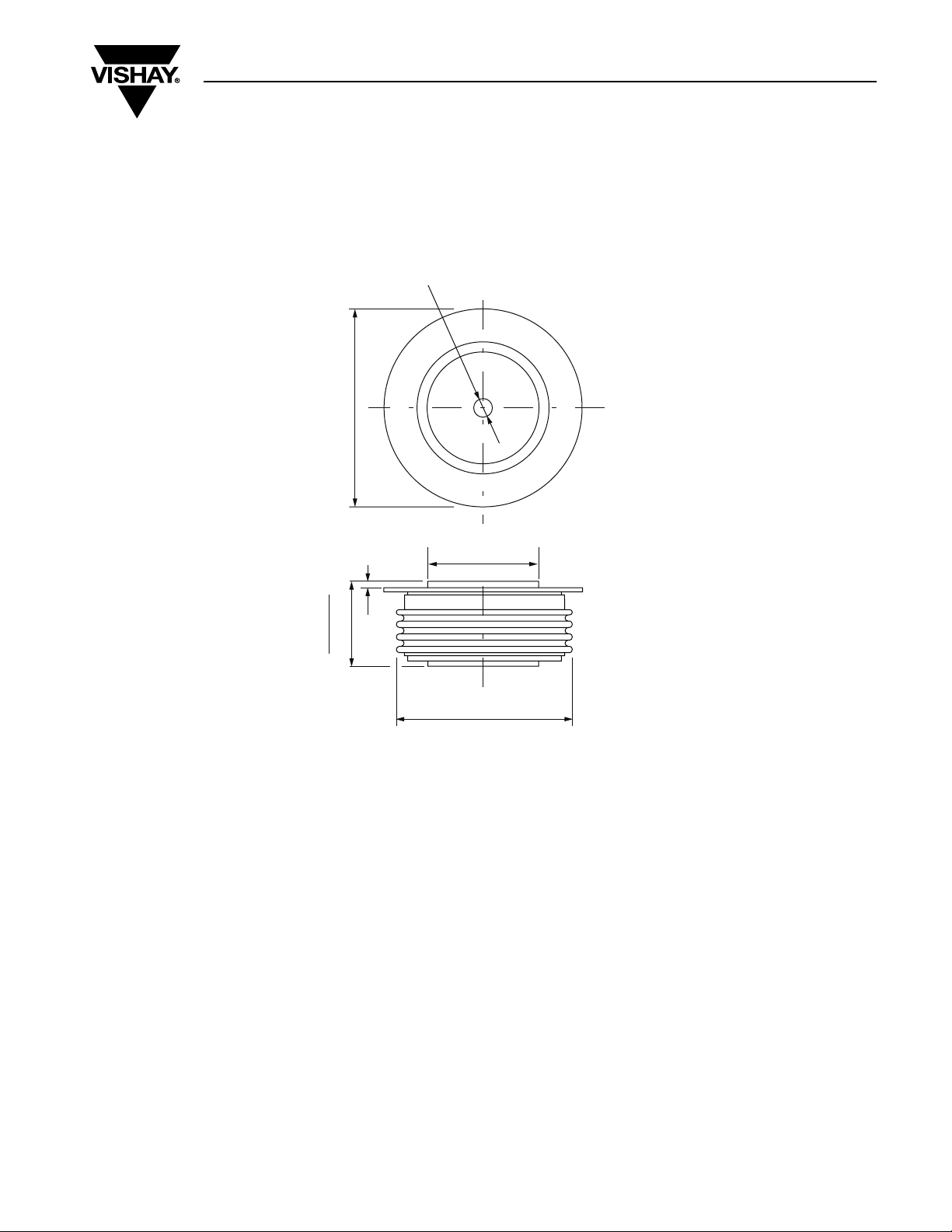
DIMENSIONS in millimeters (inches)
3.5 (0.14) DIA. NOM. x
1.8 (0.07) deep MIN. both ends
Outline Dimensions
Vishay High Power Products
DO-200AB (B-PUK)
58.5 (2.30) DIA. MAX.
0.8 (0.03)
both ends
25.4 (1)
26.9 (1.06)
Quote between upper and lower pole pieces has to be considered after
application of mounting force (see Thermal and Mechanical Specifications)
34 (1.34) DIA. MAX.
2 places
53 (2.09) DIA. MAX.
Page 7

Legal Disclaimer Notice
Vishay
Disclaimer
All product specifications and data are subject to change without notice.
Vishay Intertechnology, Inc., its affiliates, agents, and employees, and all persons acting on its or their behalf
(collectively, “Vishay”), disclaim any and all liability for any errors, inaccuracies or incompleteness contained herein
or in any other disclosure relating to any product.
Vishay disclaims any and all liability arising out of the use or application of any product described herein or of any
information provided herein to the maximum extent permitted by law. The product specifications do not expand or
otherwise modify Vishay’s terms and conditions of purchase, including but not limited to the warranty expressed
therein, which apply to these products.
No license, express or implied, by estoppel or otherwise, to any intellectual property rights is granted by this
document or by any conduct of Vishay.
The products shown herein are not designed for use in medical, life-saving, or life-sustaining applications unless
otherwise expressly indicated. Customers using or selling Vishay products not expressly indicated for use in such
applications do so entirely at their own risk and agree to fully indemnify Vishay for any damages arising or resulting
from such use or sale. Please contact authorized Vishay personnel to obtain written terms and conditions regarding
products designed for such applications.
Product names and markings noted herein may be trademarks of their respective owners.
 Loading...