

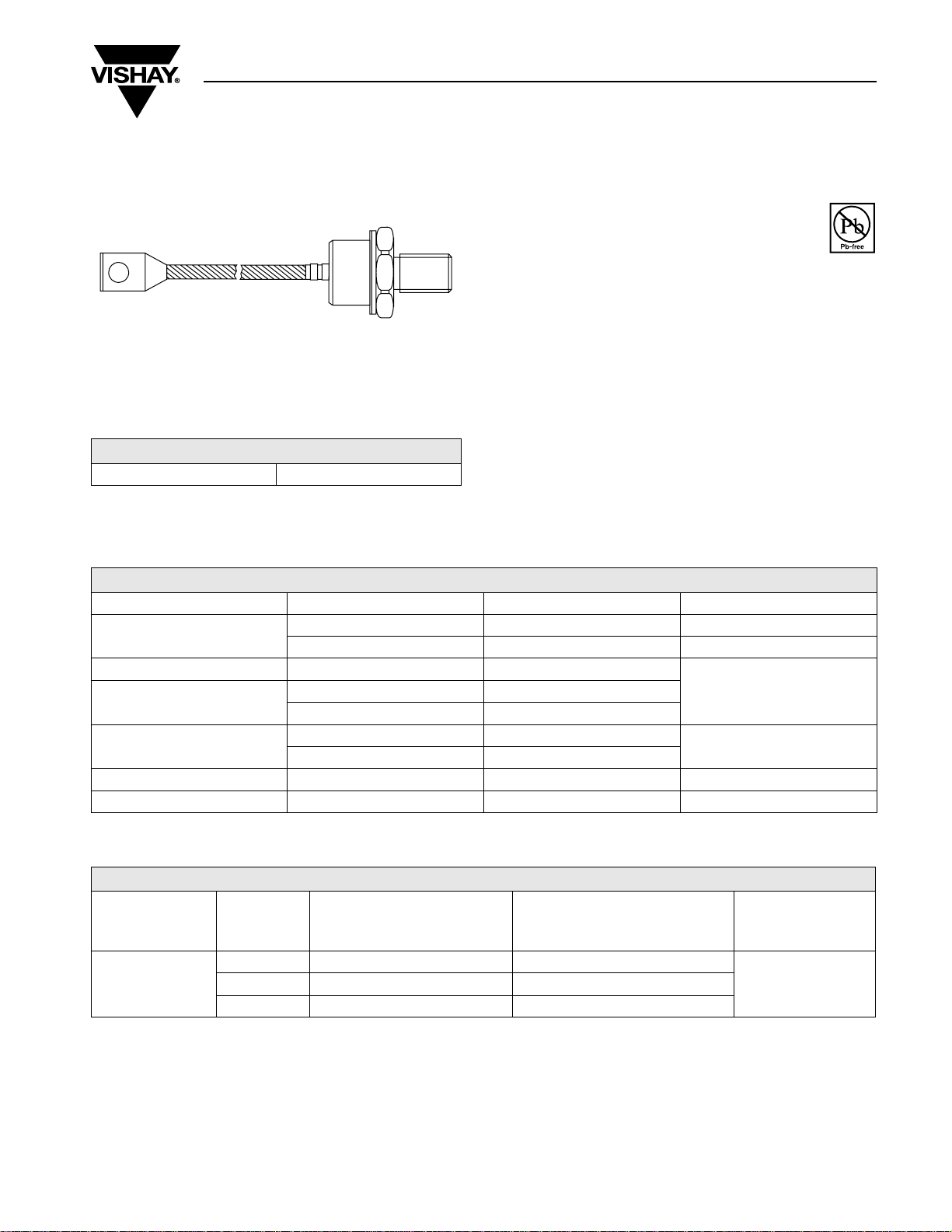
DO-205AB (DO-9)
PRODUCT SUMMARY
I
F(AV)
Vishay High Power Products
Standard Recovery Diodes
(Stud Version), 400 A
FEATURES
• Wide current range
• High voltage ratings up to 2400 V
• High surge current capabilities
• Stud cathode and stud anode version
• Standard JEDEC types
• Compression bonded encapsulations
• Lead (Pb)-free
• Designed and qualified for industrial level
TYPICAL APPLICATIONS
• Converters
400 A
• Power supplies
• Machine tool controls
• High power drives
• Medium traction applications
SD400N/R Series
RoHS
COMPLIANT
MAJOR RATINGS AND CHARACTERISTICS
PARAMETER TEST CONDITIONS VALUES UNITS
I
F(AV)
I
F(RMS)
I
FSM
2
I
t
V
RRM
T
J
T
C
50 Hz 8250
60 Hz 8640
50 Hz 340
60 Hz 311
Range 1600 to 2400 V
480 A
120 °C
630
- 40 to 190 °C
ELECTRICAL SPECIFICATIONS
VOLTAGE RATINGS
V
TYPE NUMBER
SD400N/R
, MAXIMUM REPETITIVE
VOLTAGE
CODE
16 1600 1700
24 2400 2500
RRM
PEAK REVERSE VOLTAGE
V
V
, MAXIMUM NON-REPETITIVE
RSM
PEAK REVERSE VOLTAGE
V
I
AT T
A
kA2s
MAXIMUM
RRM
= TJ MAXIMUM
J
mA
1520 2000 2100
SD400N/R Series
Vishay High Power Products
Standard Recovery Diodes
(Stud Version), 400 A
FORWARD CONDUCTION
PARAMETER SYMBOL TEST CONDITIONS VALUES UNITS
400 A
Maximum average forward current
at case temperature
Maximum RMS forward current I
Maximum peak, one-cycle forward,
non-repetitive surge current
Maximum I
Maximum I
2
t for fusing I2t
2
√t for fusing I2√t t = 0.1 to 10 ms, no voltage reapplied 3400 kA2√s
Low level value of threshold voltage V
High level value of threshold voltage V
Low level value of forward
slope resistance
High level value of forward
slope resistance
Maximum forward voltage drop V
I
F(AV)
F(RMS)
I
FSM
F(TO)1
F(TO)2
r
f1
r
f2
FM
180° conduction, half sine wave
DC at 110 °C case temperature 630
t = 10 ms
t = 8.3 ms 8640
t = 10 ms
t = 8.3 ms 7270
t = 10 ms
t = 8.3 ms 311
t = 10 ms
t = 8.3 ms 220
(16.7 % x π x I
= TJ maximum
T
J
(I > π x I
(16.7 % x π x I
= TJ maximum
T
J
(I > π x I
No voltage
reapplied
100 % V
RRM
reapplied
No voltage
Sinusoidal half wave,
initial T
= TJ maximum
J
reapplied
100 % V
RRM
reapplied
< I < π x I
F(AV)
), TJ = TJ maximum 0.85
F(AV)
< I < π x I
F(AV)
), TJ = TJ maximum 0.51
F(AV)
F(AV)
F(AV)
),
),
Ipk = 1500 A, TJ = TJ maximum,
= 10 ms sinusoidal wave
t
p
120 °C
480 A
100 °C
8250
6940
340
241
0.80
0.55
1.62 V
kA
mΩ
A
2
s
V
THERMAL AND MECHANICAL SPECIFICATIONS
PARAMETER SYMBOL TEST CONDITIONS VALUES UNITS
Maximum junction operating
temperature range
Maximum storage temperature range T
Maximum thermal resistance,
junction to case
Maximum thermal resistance,
case to heatsink
Maximum allowed
mounting torque ± 10 %
Approximate weight 250 g
Case style See dimensions (link at the end of datasheet) DO-205AB (DO-9)
R
R
T
J
Stg
thJC
thCS
- 40 to 190
°C
- 55 to 200
DC operation 0.11
K/W
Mounting surface, smooth, flat and greased 0.04
Not-lubricated threads 27 Nm
SD400N/R Series
Standard Recovery Diodes
Vishay High Power Products
(Stud Version), 400 A
ΔR
Note
• The table above shows the increment of thermal resistance R
CONDUCTION
thJC
CONDUCTION ANGLE SINUSOIDAL CONDUCTION RECTANGULAR CONDUCTION TEST CONDITIONS UNITS
180° 0.020 0.013
120° 0.023 0.023
T
90° 0.029 0.031
= TJ maximum K/W
J
60° 0.042 0.044
30° 0.073 0.074
when devices operate at different conduction angles than DC
thJC
190
180
SD 4 0 0N / R Se r ie s
R (DC ) = 0.11 K/ W
thJC
170
160
Cond uction Angle
150
140
130
120
110
Maximum Allowab le Case Temp erature (°C)
0 50 100 150 200 250 300 350 400 450
30°
60°
90°
Average Forward Current (A)
120°
180°
190
180
SD 40 0 N / R Se r i e s
R (DC) = 0.11 K/W
thJC
170
160
150
Conduction Period
140
130
120
110
100
Maximum Allowable Case Temperature (°C)
0 100 200 300 400 500 600 700
30°
60°
90°
120°
180°
Average Forward Current (A)
DC
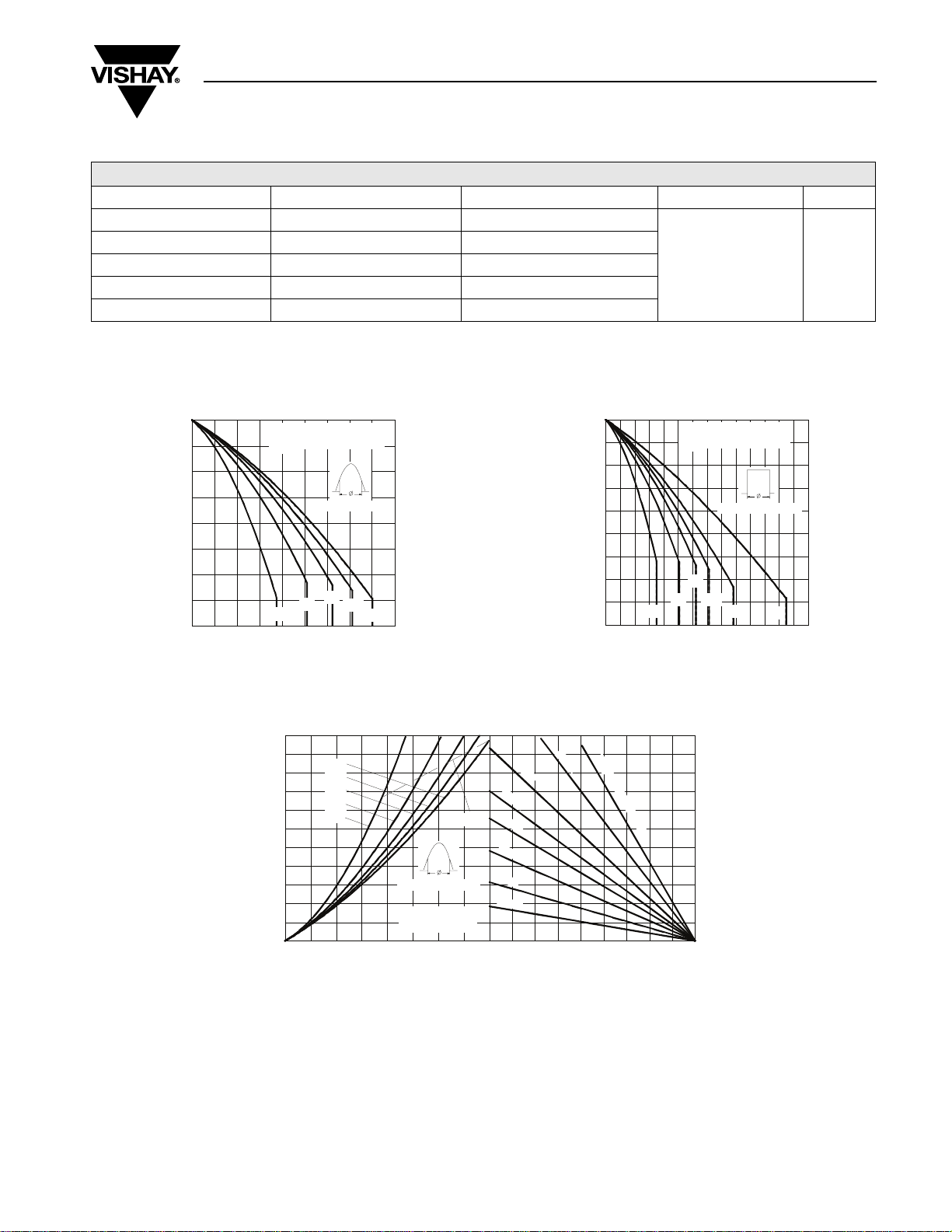
Fig. 1 - Current Ratings Characteristics Fig. 2 - Current Ratings Characteristics
550
0
500
450
400
350
300
250
200
150
100
50
0
Maximum Average Forward Power Loss (W)
180°
120°
90°
60°
30°
Cond uction Angle
SD 40 0N / R Se r i e s
T = 19 0 °C
J
0
50 100 150 200 250 300 350 4 00
Average Forward Current (A)
0
.
3
K
0
.
RM S Li mi t
4
K
/
0
.6
K
/
1
K
/
W
1
.
8
K
/
10 30 50 70 90 110 130 150 170 19 0
Maximum Allowable Ambient Tem perat ure (°C)
.
R
1
K
t
h
0
.
2K
/
W
W
W
W
/
W
S
/
W
A
=
0
.
0
4
K
/
W
D
e
l
t
a
R
Fig. 3 - Forward Power Loss Characteristics
SD400N/R Series
Vishay High Power Products
800
700
600
500
400
300
200
100
Maximum Averag e Forward Pow er Loss (W)
8000
At Any Rated Load Condition And With
Rated V Applied Following Surge.
7000
RRM
6000
5000
4000
3000
SD 40 0N / R Se r i e s
Peak Half Sine Wave Forward Current (A)
2000
110100
Numb er Of Eq ua l Amp litud e Half Cyc le Cu rren t Pulses (N)
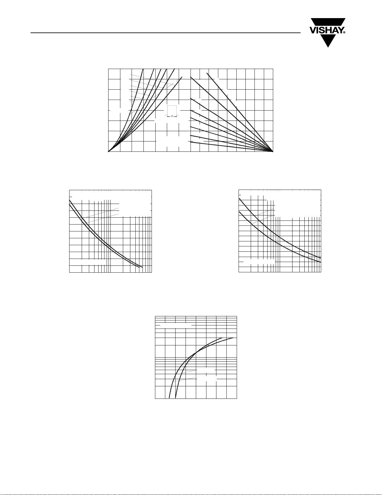
Fig. 5 - Maximum Non-Repetitive Surge Current Fig. 6 - Maximum Non-Repetitive Surge Current
DC
180°
120°
90°
60°
30°
RM S Li m it
0
0 100 200 300 400 500 600 700
Average Forward Current (A)
Init ial T = 190°C
J
@ 60 Hz 0.0083 s
@ 50 Hz 0.0100 s
Standard Recovery Diodes
(Stud Version), 400 A
R
t
h
0
.
S
1
A
K
/
=
W
0
.
0
4
K
/
W
Pea k Half Sine Wave Forwa rd Current (A)
9000
8000
7000
6000
5000
4000
3000
2000
1000
D
e
0
.
2
K
/
W
0
.
3
K/
W
0
.
4
K
/
Conduc tion Period
SD 4 0 0N / R Se r ie s
T = 190°C
J
W
0
.
6
K
/
W
1
K
/
W
1
.
8
K
/
W
10 30 50 70 90 110 13 0 150 170 190
Maximum Allowable Ambient Temperature (°C)
Fig. 4 - Forward Power Loss Characteristics
l
t
a
R
Maximum Non Repetitive Surge Current
Versus Pulse Train Durat ion.
Init ial T = 190° C
J
No Volt ag e Rea pp lie d
Rated V Reapplied
RRM
SD 4 0 0N / R Se r i e s
0.01 0.1 1
Pulse Tra in Du ra t io n (s)
10000
SD 40 0N / R Se r i e s
1000
T = 25 ° C
J
T = 19 0 ° C
J
Instantaneous Forward Current (A)
100
0.5 1 1.5 2 2.5
In st a nt a n e o us Fo rw a rd V olt a g e ( V)
Fig. 7 - Forward Voltage Drop Characteristics
SD400N/R Series
Standard Recovery Diodes
1
thJC
0.01
Transient Thermal Impedance Z (K/ W)
0.001
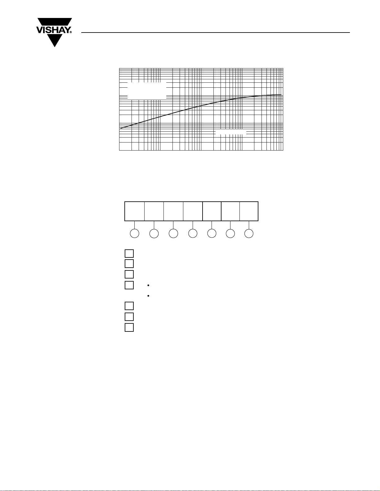
ORDERING INFORMATION TABLE
Device code
St e a d y St a t e V a l u e :
R = 0.11 K/ W
0.1
thJC
(DC Operation)
0.001 0.01 0.1 1 10
SD 40 0 N 24 P C
(Stud Version), 400 A
Sq u a re Wa v e Pu l se D u r a t i o n ( s )
Fig. 8 - Thermal Impedance Z
SD 40 0 N / R Se r i e s
Characteristic
thJC
Vishay High Power Products
51324
67
1 - Diode
2 - Essential part number
3 - 0 = Standard recovery
4 - N = Stud normal polarity (cathode to stud)
R = Stud reverse polarity (anode to stud)
5 - Voltage code x 100 = V
(see Voltage Ratings table)
RRM
6 - P = Stud base DO-205AB (DO-9) 3/4" 16UNF-2A
7
- C = Ceramic housing
For metric device M16 x 1.5 contact factory
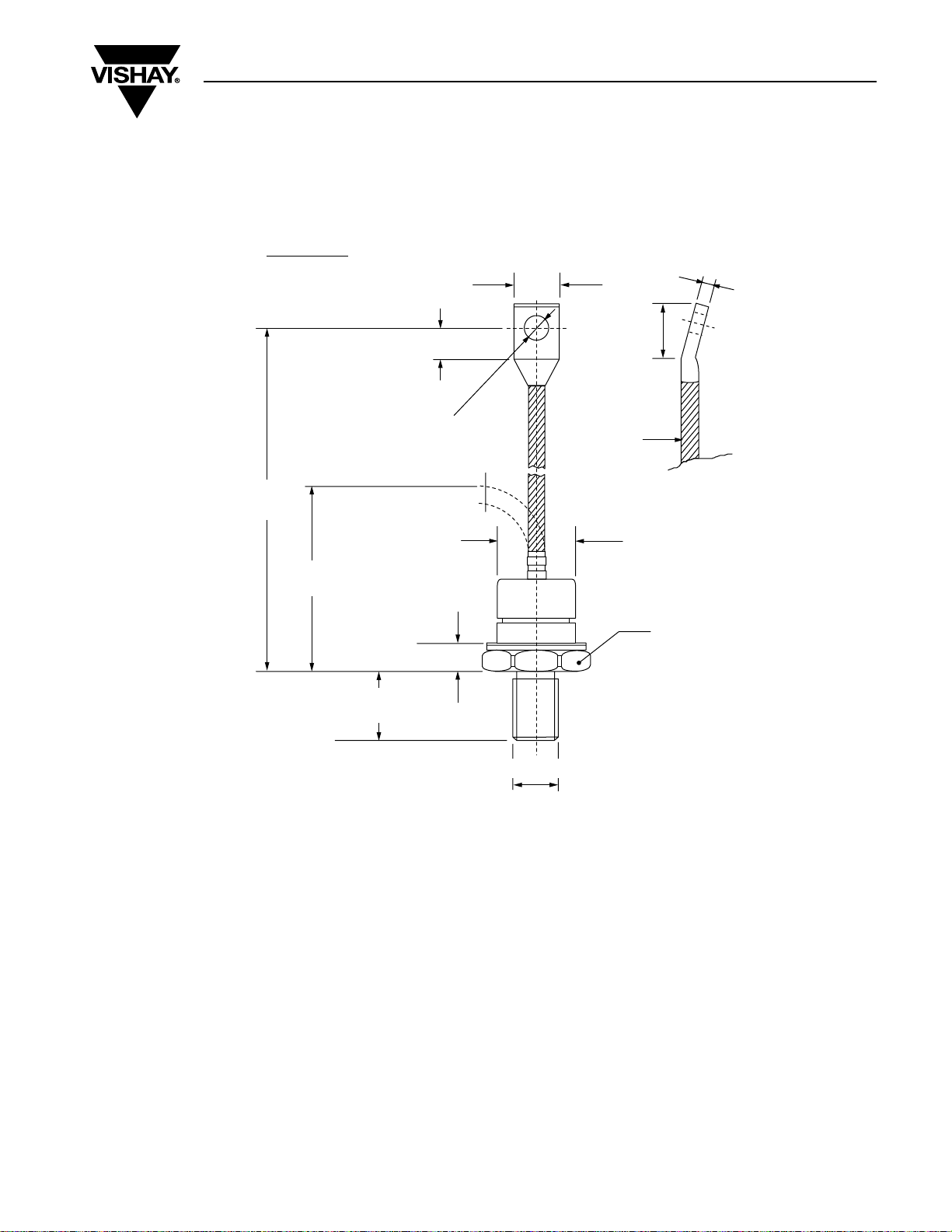
DIMENSIONS in millimeters (inches)
Outline Dimensions
Vishay High Power Products
DO-205AB (DO-9)
Ceramic housing
210 (8.27)
± 10 (0.39)
82 (3.23)
MIN.
DIA. 8.5 (0.33) NOM.
DIA. 27.5
(1.08) MAX.
21 (0.82)
MAX.
9.5 (0.37) MIN.
16 (0.63)
MAX.
19 (0.75)
MAX.
39 (1.53)
MAX.
C.S. 35 mm
(0.054 s.i.)
SW 32
4 (0.16)
MAX.
2
3/4"-16UNF-2A*
*For metric device: M16 x 1.5
contact factory

Legal Disclaimer Notice
Vishay
Disclaimer
All product specifications and data are subject to change without notice.
Vishay Intertechnology, Inc., its affiliates, agents, and employees, and all persons acting on its or their behalf
(collectively, “Vishay”), disclaim any and all liability for any errors, inaccuracies or incompleteness contained herein
or in any other disclosure relating to any product.
Vishay disclaims any and all liability arising out of the use or application of any product described herein or of any
information provided herein to the maximum extent permitted by law. The product specifications do not expand or
otherwise modify Vishay’s terms and conditions of purchase, including but not limited to the warranty expressed
therein, which apply to these products.
No license, express or implied, by estoppel or otherwise, to any intellectual property rights is granted by this
document or by any conduct of Vishay.
The products shown herein are not designed for use in medical, life-saving, or life-sustaining applications unless
otherwise expressly indicated. Customers using or selling Vishay products not expressly indicated for use in such
applications do so entirely at their own risk and agree to fully indemnify Vishay for any damages arising or resulting
from such use or sale. Please contact authorized Vishay personnel to obtain written terms and conditions regarding
products designed for such applications.
Product names and markings noted herein may be trademarks of their respective owners.
 Loading...