

Page 1
Vishay High Power Products
Fast Recovery Diodes
(Hockey PUK Version), 350 A
FEATURES
• High power FAST recovery diode series
SD303C..C Series
• 1.0 to 2.0 µs recovery time
• High voltage ratings up to 2500 V
• High current capability
• Optimized turn-on and turn-off characteristics
DO-200AA
• Low forward recovery
• Fast and soft reverse recovery
• Press PUK encapsulation
• Case style conform to JEDEC DO-200AA
• Maximum junction temperature 125 °C
PRODUCT SUMMARY
I
F(AV)
350 A
• Lead (Pb)-free
TYPICAL APPLICATIONS
• Snubber diode for GTO
• High voltage freewheeling diode
• Fast recovery rectifier applications
MAJOR RATINGS AND CHARACTERISTICS
PARAMETER TEST CONDITIONS VALUES UNITS
I
F(AV)
I
F(RMS)
I
FSM
2
I
t
V
RRM
t
rr
T
J
T
hs
T
hs
50 Hz 5770
60 Hz 6040
50 Hz 166
60 Hz 152
Range 400 to 2500 V
T
J
350 A
55 °C
550 A
25 °C
1.0 to 2.0 µs
25
- 40 to 125
A
kA2s
°C
RoHS
COMPLIANT
Document Number: 93174 For technical questions, contact: ind-modules@vishay.com
Revision: 04-Aug-08 1
www.vishay.com
Page 2
SD303C..C Series
Vishay High Power Products
Fast Recovery Diodes
(Hockey PUK Version), 350 A
ELECTRICAL SPECIFICATIONS
VOLTAGE RATINGS
V
, MAXIMUM REPETITIVE PEAK
TYPE NUMBER
VOLTAGE
CODE
RRM
AND OFF-STATE VOLTAGE
V
04 400 500
SD303C..S10C
08 800 900
10 1000 1100
12 1200 1300
SD303C..S15C
14 1400 1500
16 1600 1700
SD303C..S20C
20 2000 2100
25 2500 2600
FORWARD CONDUCTION
PARAMETER SYMBOL TEST CONDITIONS VALUES UNITS
Maximum average forward current
at heatsink temperature
Maximum RMS current I
F(RMS)
Maximum peak, one-cycle ,
non-repetitive forward current
Maximum I
Maximum I
2
t for fusing I2t
2
√t for fusing I2√t t = 0.1 to 10 ms, no voltage reapplied 1660 kA2√s
Low level value of threshold voltage V
High level value of threshold voltage V
Low level of forward slope resistance r
High level of forward slope resistance r
Maximum forward voltage drop V
I
F(AV)
I
FSM
F(TO)1
F(TO)2
180° conduction, half sine wave
Double side (single side) cooled
25 °C heatsink temperature double side cooled 550
t = 10 ms
t = 8.3 ms 6040
t = 10 ms
t = 8.3 ms 5080
t = 10 ms
t = 8.3 ms 152
t = 10 ms
t = 8.3 ms 107
(16.7 % x π x I
(I > π x I
(16.7 % x π x I
f1
(I > π x I
f2
Ipk = 1100 A, TJ = 25 °C; tp = 10 ms sinusoidal wave 2.26 V
FM
No voltage
reapplied
100 % V
reapplied
No voltage
reapplied
100 % V
reapplied
F(AV)
), TJ = TJ maximum 1.63
F(AV)
F(AV)
), TJ = TJ maximum 0.77
F(AV)
V
RRM
RRM
< I < π x I
< I < π x I
, MAXIMUM NON-REPETITIVE
RSM
PEAK REVERSE VOLTAGE
V
Sinusoidal half wave,
initial T
= TJ maximum
J
), TJ = TJ maximum 1.14
F(AV)
), TJ = TJ maximum 1.14
F(AV)
I
MAXIMUM
RRM
= 125 °C
AT T
J
mA
35
350 (175) A
55 (75) °C
5770
4850
166
117
A
kA2s
V
mΩ
RECOVERY CHARACTERISTICS
TYPICAL VALUES
AT T
= 125 °C
J
RRM
(µs)
Q
(µC)
rr
2.4 52 33
I
(A)
I
rr
FM
t
rr
I
RM(REC)
t
Q
rr
dir
dt
Document Number: 93174
CODE
MAXIMUM VALUE
AT T
= 25 °C
J
AT 25 % I
t
rr
RRM
(µs)
TEST CONDITIONS
I
pk
SQUARE
PULSE
dI/dt
(A/µs)
V
(V)
r
t
AT 25 % I
rr
(A)
S10 1.0
S15 1.5 2.9 90 44
750 25 - 30
S20 2.0 3.2 107 46
www.vishay.com For technical questions, contact: ind-modules@vishay.com
2 Revision: 04-Aug-08
Page 3
SD303C..C Series
Fast Recovery Diodes
Vishay High Power Products
(Hockey PUK Version), 350 A
THERMAL AND MECHANICAL SPECIFICATIONS
PARAMETER SYMBOL TEST CONDITIONS VALUES UNITS
Maximum operating temperature range T
Maximum storage temperature range T
Maximum thermal resistance,
junction to heatsink
Mounting force, ± 10 % 4900 (500) N (kg)
Approximate weight 70 g
Case style See dimensions - link at the end of datasheet DO-200AA
ΔR
CONDUCTION ANGLE
Note
• The table above shows the increment of thermal resistance R
CONDUCTION
thJ-hs
SINUSOIDAL CONDUCTION RECTANGULAR CONDUCTION
SINGLE SIDE DOUBLE SIDE SINGLE SIDE DOUBLE SIDE
180° 0.010 0.011 0.008 0.008
120° 0.012 0.013 0.013 0.013
90° 0.016 0.016 0.018 0.018
60° 0.024 0.024 0.025 0.025
30° 0.042 0.042 0.042 0.042
R
J
Stg
thJ-hs
DC operation single side cooled 0.16
DC operation double side cooled 0.08
when devices operate at different conduction angles than DC
thJ-hs
- 40 to 125
- 40 to 150
TEST CONDITIONS UNITS
T
= TJ maximum K/W
J
°C
K/W
Document Number: 93174 For technical questions, contact: ind-modules@vishay.com
Revision: 04-Aug-08 3
www.vishay.com
Page 4
SD303C..C Series
Vishay High Power Products
130
120
110
100
90
80
70
60
0 20 40 60 80 100 120 140 160 180
Maximum Allowable Heatsink Temperature (°C)
Averag e Forw ard Current (A )
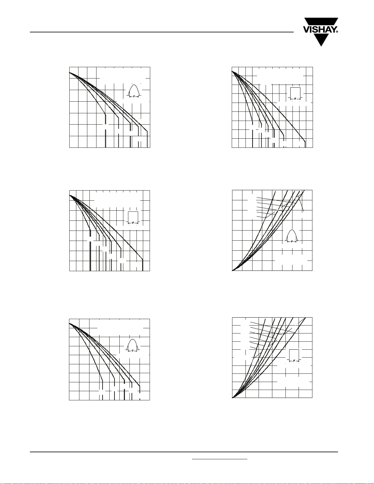
Fig. 1 - Current Ratings Characteristics
130
120
110
100
90
80
70
60
50
0 50 100 150 200 250 300
Maxim um Allowable Heatsink Temperature (°C)
Average Forward Current (A)
Fig. 2 - Current Ratings Characteristics
SD303C..C Series
(Single Side Cooled)
R (DC ) = 0 .1 6 K/ W
th J-hs
Conduction Angle
30°
60°
SD 303C ..C S eries
(Single Side Coo led )
R ( D C ) = 0 . 1 6 K /W
thJ-h s
Conduction Period
30°
60°
90°
120°
180°
90°
Fast Recovery Diodes
(Hockey PUK Version), 350 A
180°
120°
Maximum Allow able Heatsink Temperature (°C)
DC
130
120
110
100
90
80
70
60
50
40
0 100 200 300 400 500 600
SD303C..C Series
(D ou ble Side C o oled )
R (DC) = 0.08 K/W
th J-hs
Conduction Period
30°
60°
90°
120°
180° DC
Average Forward Current (A)
Fig. 4 - Current Ratings Characteristics
800
700
600
500
400
300
200
100
0
Maximum Average Forward Power Loss (W)
180°
120°
90°
60°
30°
0 50 100 150 200 250 300 350 400
Average Forward Current (A)
RMS Limit
Conduction Angle
SD 3 0 3C ..C Se ries
T = 125°C
J
Fig. 5 - Forward Power Loss Characteristics
130
120
110
100
90
80
70
60
50
40
0 50 100 150 200 250 300 350 400
Maximum Allow able Heatsink Tem perature (°C)
SD303C ..C Se ries
(Double Side Cooled)
R (DC ) = 0 .08 K/ W
thJ-h s
Conduction Angle
90°
60°
30°
Average Forward Current (A)
Fig. 3 - Current Ratings Characteristics
120°
180°
1000
900
800
700
600
500
400
300
200
100
Maximum Average Forward Power Loss (W)
DC
180°
120°
90°
60°
30°
RMS Lim it
Conduction Period
SD 30 3 C ..C Se ries
T = 1 25°C
J
0
0100200300400500600
Average Forward Current (A)
Fig. 6 - Forward Power Loss Characteristics
www.vishay.com For technical questions, contact: ind-modules@vishay.com
Document Number: 93174
4 Revision: 04-Aug-08
Page 5

SD303C..C Series
Fast Recovery Diodes
(Hockey PUK Version), 350 A
5500
At Any Rated Load Condition And W ith
Rated V Applied Following Surge.
5000
4500
4000
3500
3000
2500
SD 30 3C ..C Se ries
Peak Half Sine Wave Forward Current (A)
2000
N u m b e r O f E q ua l Am p litu d e H a lf C ycle C urr ent Pu ls es (N )
Fig. 7 - Maximum Non-Repetitive Surge Current
6000
M a x im um N on Re p et itive S u rg e C urren t
5500
5000
4500
4000
3500
3000
2500
2000
Peak Half Sine Wave Forward C urrent (A)
1500
0.01 0.1 1
Fig. 8 - Maximum Non-Repetitive Surge Current
RRM
Initia l T = 1 2 5°C
J
@ 60 H z 0.0083 s
@ 50 H z 0.0100 s
Single and Double Side Cooled
V e r su s P u ls e T r a i n D u r a t io n .
SD303C..C Series
Pulse Train Duration (s)
Initia l T = 1 25 ° C
N o V o lt a g e R e a p p l ie d
Ra ted V Rea p p lie d
J
RRM
Single and Double Side Cooled
Vishay High Power Products
10000
SD303C ..C Series
1000
100
Insta n tan eo us Fo rw a rd C urre n t (A )
10
001011
0123 45 6 78
Instantaneous Forward Voltage (V)
Fig. 9 - Forward Voltage Drop Characteristics
1
Steady S tate Va lu e
R = 0.16 K/W
thJ-h s
(Sin g le Sid e C oole d)
thJ-h s
R = 0.08 K/W
thJ-h s
0.1
(D oub le Sid e C ooled )
(D C O p e ration )
0.01
0.001
Transient Therm a l Impedan ce Z (K/W )
0.0001 0.001 0.01 0.1 1 10 100
Squa re W a ve Pulse D ur atio n ( s)
Fig. 10 - Thermal Impedance Z
T = 25 °C
J
T = 12 5 ° C
J
SD 30 3 C ..C Se ries
Characteristic
thJ-hs
120
V
100
80
60
40
Forw ard Recovery (V)
20
0
FP
0 200 400 600 800 1000 1200 1400 1600 1800 2000
I
Rate Of f Fall O f Forw ard C urren t d i/dt (A /u sec)
T = 125°C
J
T = 25°C
J
SD 303C ..S20C Se ries
Fig. 11 - Typical Forward Recovery Characteristics
Document Number: 93174 For technical questions, contact: ind-modules@vishay.com
www.vishay.com
Revision: 04-Aug-08 5
Page 6

SD303C..C Series
Vishay High Power Products
2.8
SD 303C ..S1 0C Se ries
2.6
2.4
2.2
1.8
Maximum Reverse Recovery Time - Trr (µs)
1.6
Rate Of Fall Of Forward Curre nt - di/dt (A/µs)
Fig. 12 - Recovery Time Characteristics
140
130
120
110
100
90
80
70
60
50
40
30
20
10
Maximum Reverse Recovery Charge - Qrr (µC)
Ra te O f Fa ll Of Fo rwar d Cu rrent - d i/dt (A /µs)
Fig. 13 - Recovery Charge Characteristics
T = 1 25 °C, V = 30V
J
2
SD303C ..S10C Series
T = 125 °C , V = 30V
J
0 20406080100
r
I = 750 A
FM
Squa re Pulse
I = 7 50 A
FM
Sq u a re Pul se
400 A
200 A
r
400 A
200 A
Fast Recovery Diodes
(Hockey PUK Version), 350 A
00101
Rate Of Fall Of Forward C urrent - di/dt (A/µs)
Fig. 15 - Recovery Time Characteristics
Ra te O f Fa ll O f Fo r w a rd C ur r en t - di/ dt (A/ µs )
Fig. 16 - Recovery Charge Characteristics
3.6
3.2
2.8
2.4
M ax im um R eve rse Reco ve ry Time - T rr (µs)
1.6
170
160
150
140
130
120
110
100
90
80
70
60
50
M axim um Reverse Recovery Charge - Qrr (µC)
SD303C ..S15C Series
T = 125 °C, V = 30V
J
I = 75 0 A
FM
Sq ua re P u ls e
2
I = 75 0 A
FM
Sq ua re P u ls e
400 A
200 A
SD303C ..S15C Series
T = 125 °C , V = 30V
J
10 20 30 4 0 50 60 70 80 90 100
r
400 A
200 A
00101
r
100
90
80
70
60
50
40
30
20
M a xim u m Rev erse R e co v ery C u rren t - Irr (A )
20 30 40 5 0 60 70 80 90 10 0
Rate O f Fa ll Of F orwa rd Cur ren t - di/d t (A/µs )
I = 75 0 A
FM
Square Pulse
400 A
200 A
SD 303C..S10C Serie s
T = 1 2 5 °C , V = 3 0 V
J
r
Fig. 14 - Recovery Current Characteristics
130
120
110
100
90
80
70
60
50
40
30
20
10
M a xim u m R ev erse Re co v ery C urre n t - Irr (A )
10 20 30 40 50 60 70 80 90 1 00
Rate Of Fall Of Forward Current - di/d t (A/µs)
I = 7 50 A
FM
Sq ua re P u lse
400 A
200 A
SD 3 03C ..S15 C Se ries
T = 12 5 °C, V = 30V
J
r
Fig. 17 - Recovery Current Characteristics
www.vishay.com For technical questions, contact: ind-modules@vishay.com
Document Number: 93174
6 Revision: 04-Aug-08
Page 7

SD303C..C Series
Fast Recovery Diodes
Vishay High Power Products
(Hockey PUK Version), 350 A
3.6
3.4
3.2
3
2.8
2.6
Max imu m Re verse Recovery Time - Trr (µs)
2.4
Rate O f Fa ll O f For wa rd Curr ent - di/d t (A/µs )
SD303C..S20C Series
T = 125 ° C , V = 30V
J
400 A
200 A
r
I = 750 A
FM
Square Pulse
00101
Fig. 18 - Recovery Time Characteristics Fig. 19 - Recovery Charge Characteristics
130
120
110
100
90
80
70
60
50
40
30
20
M a x im um R ev e rse Rec o very C u rren t - Irr (A )
10 20 3 0 40 50 60 70 80 90 100
Rate Of Fall Of Forward Current - di/d t (A/µs)
I = 750 A
FM
Sq uare Pulse
400 A
200 A
SD303C ..S20C Serie s
T = 125 °C , V = 30V
J
r
300
I = 750 A
FM
250
200
150
100
50
10 20 30 4 0 50 60 70 80 90 100
Maximum Reverse Recovery Charge - Qrr (µC )
Rate Of Fall Of Forward Current - di/dt (A/µs)
Sq ua re Pulse
400 A
200 A
SD 3 03C ..S20 C Se ries
T = 1 2 5 ° C , V = 3 0 V
J
r
Fig. 20 - Recovery Current Characteristics
1E4
20 joules per pulse
10
4
2
1
1E3
0.04
0.02
1E2
0.01
Peak Forward Current (A)
tp
1E1
1E1 1E2 1E3 1E4
0.4
0.2
0.1
SD3 03C..S10C S eries
Sinuso ida l Pulse
T = 125°C, V = 1 120 V
dv/dt = 1000V/µs
RRM
J
Pulse Basewidth (µs)
2
1
0.4
0.2
0.1
SD303C ..S10C Series
Tra pe zoid al Pul se
T = 125°C , V = 1120V
tp
dv/dt = 1000V/µs; di/dt=50A/µs
RRM
J
1E1 1E2 1E3 1E4
Pulse Basewidth (µs)
10
4
20 jo u les p er pulse
Fig. 21 - Maximum Total Energy Loss Per Pulse Characteristics
Document Number: 93174 For technical questions, contact: ind-modules@vishay.com
www.vishay.com
Revision: 04-Aug-08 7
Page 8

SD303C..C Series
Vishay High Power Products
1E4
10
4
2
1
1E3
1E2
Peak Forw ard Current (A)
1E1
1E1 1E2 1E 3 1E4
SD303C..S15C Series
Sinuso idal Pulse
T = 12 5°C, V = 1760 V
tp
dv/dt = 1000V/µs
1E4
1E3
1E2
Peak Forw ard C urrent (A)
1E1
1E1 1E2 1E3 1E4
0.04
SD303C..S20C Series
Sinuso ida l Pulse
T = 125°C, V = 1760V
tp
dv/dt = 1000V/µs
0.4
0.2
0.1
0.04
0.02
RRM
J
Pulse Basew idth (µs)
Fig. 22 - Maximum Total Energy Loss Per Pulse Characteristics
2
1
0.4
0.2
0.1
J
RRM
Pulse Basew id th (µ s)
10
4
Fast Recovery Diodes
(Hockey PUK Version), 350 A
20 jo ules p er pu lse
1E1 1E2 1E3 1E4
20 joules per pulse
1E1 1 E2 1E3 1E4
0.2
SD303C..S15C Series
Trapezoidal Pulse
T = 125°C, V = 1760V
J
tp
dv/dt = 1000V/µs; di/dt=50A/µs
Pulse Basewidth (µs)
0.2
SD303C..S20C Series
Trapezoidal Pulse
T = 125°C, V = 1760V
J
tp
dv/dt = 1000V/µs; di/dt=50A/µs
Pulse Basewidth (µs)
RRM
RRM
0.4
0.4
20 jo ules per p ulse
10
4
2
1
20 jo ul es per p ulse
10
4
2
1
Fig. 23 - Maximum Total Energy Loss Per Pulse Characteristics
www.vishay.com For technical questions, contact: ind-modules@vishay.com
Document Number: 93174
8 Revision: 04-Aug-08
Page 9

SD303C..C Series
(Hockey PUK Version), 350 A
ORDERING INFORMATION TABLE
Device code
SD 30 3 C 25 S20 C
1 - Diode
2 - Essential part number
3 - 3 = Fast recovery
4 - C = Ceramic PUK
5 - Voltage code x 100 = V
6 -t
7 - C = PUK case DO-200AA
Fast Recovery Diodes
51324
RRM
code (see Recovery Characteristics table)
rr
Vishay High Power Products
67
(see Voltage Ratings table)
Document Number: 93174 For technical questions, contact: ind-modules@vishay.com
Revision: 04-Aug-08 9
www.vishay.com
Page 10

DIMENSIONS in millimeters (inches)
3.5 (0.14) ± 0.1 (0.004) DIA. NOM. x
1.8 (0.07) deep MIN. both ends
Outline Dimensions
Vishay High Power Products
DO-200AA
42 (1.65) DIA. MAX.
19 (0.75) DIA. MAX.
2 places
38 (1.50) DIA. MAX.
Quote between upper and lower pole pieces has to be considered after
application of mounting force (see Thermal and Mechanical Specifications)
0.3 (0.01) MIN.
both ends
14.4 (0.57)
13.7 (0.54)
Document Number: 95248 For technical questions concerning discrete products, contact: diodes-tech@vishay.com
Revision: 06-Nov-07 For technical questions concerning module products, contact: ind-modules@vishay.com
www.vishay.com
1
Page 11

Legal Disclaimer Notice
Vishay
Notice
The products described herein were acquired by Vishay Intertechnology, Inc., as part of its acquisition of
International Rectifier’s Power Control Systems (PCS) business, which closed in April 2007. Specifications of the
products displayed herein are pending review by Vishay and are subject to the terms and conditions shown below.
Specifications of the products displayed herein are subject to change without notice. Vishay Intertechnology, Inc., or
anyone on its behalf, assumes no responsibility or liability for any errors or inaccuracies.
Information contained herein is intended to provide a product description only. No license, express or implied, by
estoppel or otherwise, to any intellectual property rights is granted by this document. Except as provided in Vishay's
terms and conditions of sale for such products, Vishay assumes no liability whatsoever, and disclaims any express
or implied warranty, relating to sale and/or use of Vishay products including liability or warranties relating to fitness
for a particular purpose, merchantability, or infringement of any patent, copyright, or other intellectual property right.
The products shown herein are not designed for use in medical, life-saving, or life-sustaining applications.
Customers using or selling these products for use in such applications do so at their own risk and agree to fully
indemnify Vishay for any damages resulting from such improper use or sale.
®
International Rectifier
are registered trademarks of International Rectifier Corporation in the U.S. and other countries. All other product
names noted herein may be trademarks of their respective owners.
, IR®, the IR logo, HEXFET®, HEXSense®, HEXDIP®, DOL®, INTERO®, and POWIRTRAIN
®
Document Number: 99901 www.vishay.com
Revision: 12-Mar-07 1
 Loading...