

S593T/S593TR/S593TRW
Vishay Telefunken
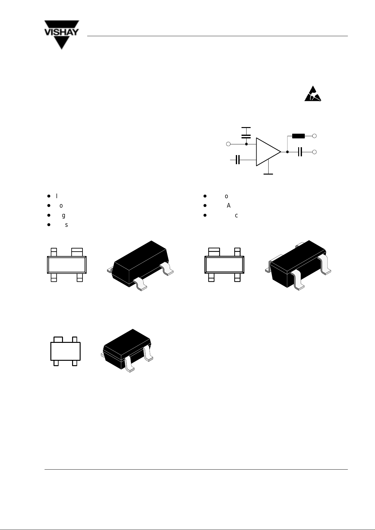
MOSMIC for TV–Tuner Prestage with 5 V Supply
Voltage
MOSMIC - MOS Monolithic Integrated Circuit Electrostatic sensitive device.
Observe precautions for handling.
Applications
Low noise gain controlled input stages in UHF-and
VHF- tuner with 5 V supply voltage.
Features
D
Integrated gate protection diodes
D
Low noise figure
D
High gain
D
Biasing network on chip
C block
AGC
RF in
C block
D
Improved cross modulation at gain reduction
D
High AGC-range
D
SMD package
G2
G1
S
RFC
D
C block
V
DD
RF out
94 9296
21
94 9279
13 579
43
S593T Marking: 593
Plastic case (SOT 143)
1 = Source, 2 = Drain, 3 = Gate 2, 4 = Gate 1
2
1
13 56613 654
34
S593TRW Marking: W93
Plastic case (SOT 343R)
1 = Source, 2 = Drain, 3 = Gate 2, 4 = Gate 1
21
94 9278
95 10831
43
S593TR Marking: 93R
Plastic case (SOT 143R)
1 = Source, 2 = Drain, 3 = Gate 2, 4 = Gate 1
Document Number 85047
Rev. 3, 20-Jan-99
www.vishay.de • FaxBack +1-408-970-5600
1 (9)
S593T/S593TR/S593TRW
Vishay Telefunken
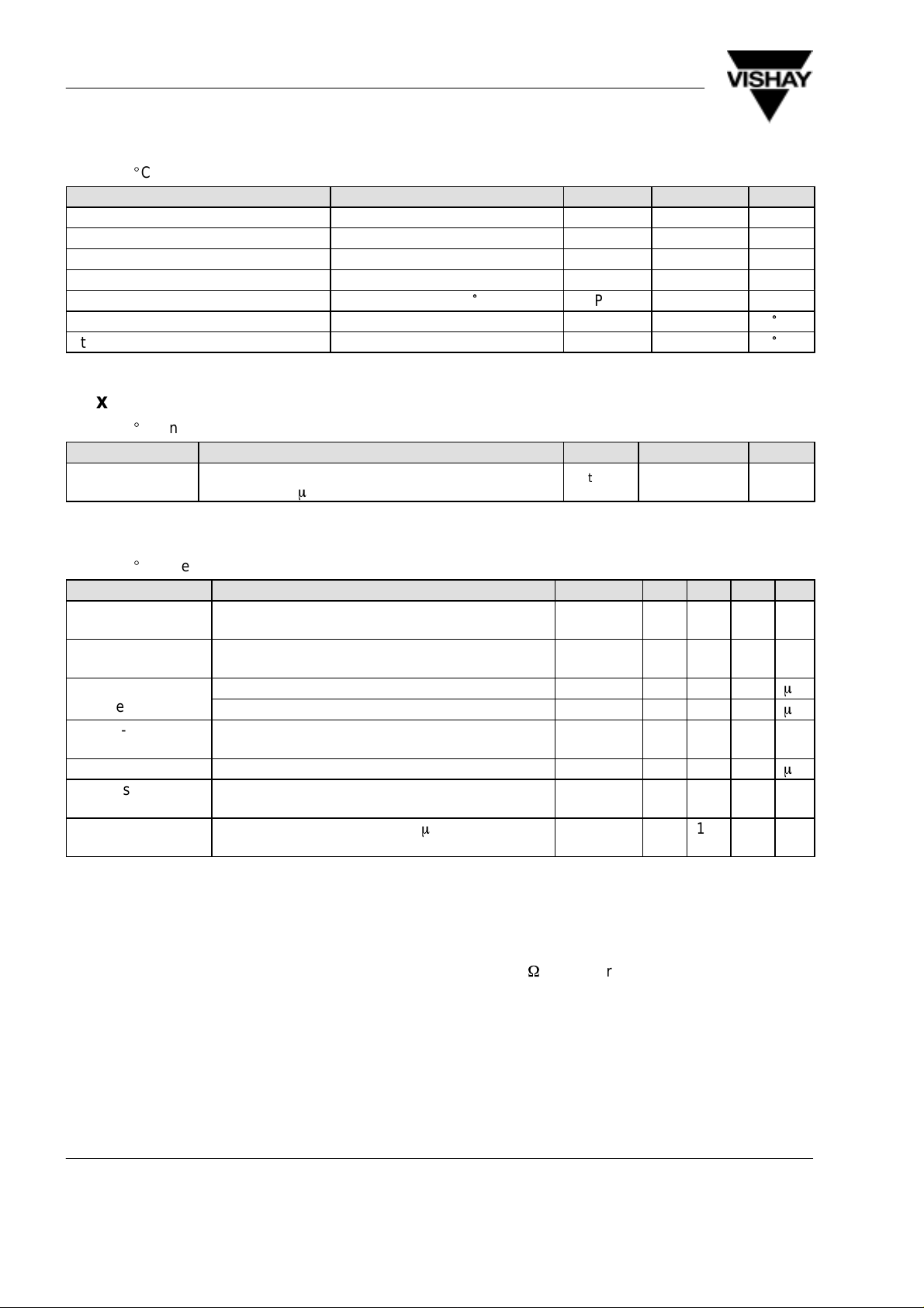
Absolute Maximum Ratings
T
= 25_C, unless otherwise specified
amb
Parameter Test Conditions Symbol Value Unit
Drain - source voltage V
Drain current I
Gate 1/Gate 2 - source peak current ±I
Gate 1/Gate 2 - source voltage ±V
Total power dissipation T
≤ 78 °C P
amb
Channel temperature T
Storage temperature range T
DS
D
G1/G2SM
G1/G2SM
tot
Ch
stg
Maximum Thermal Resistance
T
= 25_C, unless otherwise specified
amb
Parameter T est Conditions Symbol Value Unit
Channel ambient on glass fibre printed board (25 x 20 x 1.5) mm
plated with 35mm Cu
3
R
thChA
8 V
30 mA
10 mA
6 V
200 mW
150
–55 to +150
450 K/W
°
C
°
C
Electrical DC Characteristics
T
= 25_C, unless otherwise specified
amb
Parameter Test Conditions Symbol Min Typ Max Unit
Gate 1 - source
±I
G1S
= 10 mA, V
= VDS = 0 ±V
G2S
(BR)G1SS
7 10 V
breakdown voltage
Gate 2 - source
±I
G2S
= 10 mA, V
= VDS = 0 ±V
G1S
(BR)G2SS
7 10 V
breakdown voltage
Gate 1 - source +V
leakage current
Gate 2 - source
–V
±V
= 5 V, V
G1S
= 5 V, V
G1S
= 5 V, V
G2S
= VDS = 0 +I
G2S
= VDS = 0 –I
G2S
= VDS = 0 ±I
G1S
G1SS
G1SS
G2SS
leakage current
Drain current VDS = 5 V, V
Self-biased
VDS = 5 V, V
G1S
G1S
= 0, V
= nc, V
= 4 V I
G2S
= 4 V I
G2S
DSS
DSP
50 500mA
9 13 18 mA
operating current
Gate 2 - source
VDS = 5 V, V
= nc, ID = 20 mA V
G1S
G2S(OFF)
1.0 V
cut-off voltage
Caution for Gate 1 switch-off mode:
No external DC-voltage on Gate 1 in active mode!
Switch-off at Gate 1 with V
Using open collector switching transistor (inside of PLL). Insert 10 kW collector resistor.
< 0.7 V is feasible.
G1S
50
m
100mA
20 nA
A
www.vishay.de • FaxBack +1-408-970-5600
2 (9)
Document Number 85047
Rev. 3, 20-Jan-99
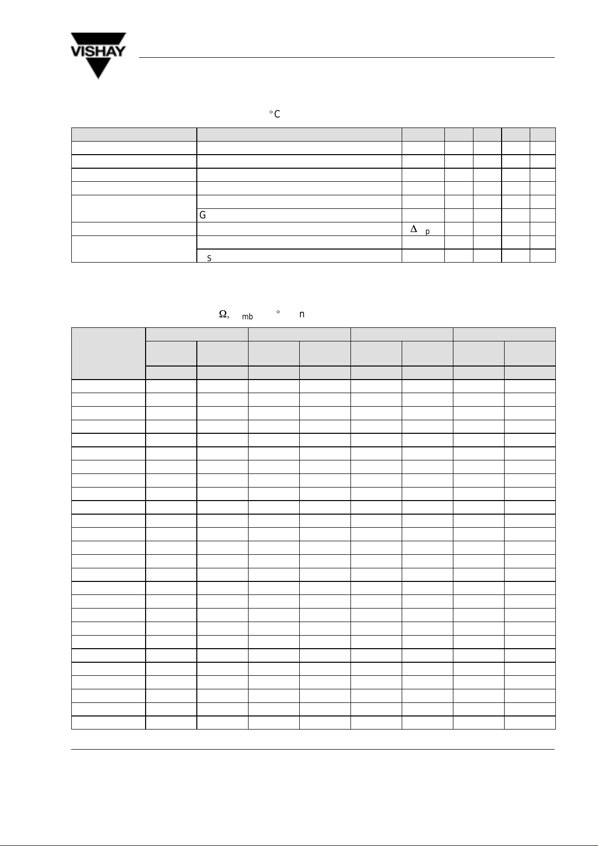
Electrical AC Characteristics
g
g
S593T/S593TR/S593TRW
Vishay Telefunken
VDS = 5 V, V
= 4 V, f = 1 MHz , T
G2S
= 25_C, unless otherwise specified
amb
Parameter Test Conditions Symbol Min Typ Max Unit
Forward transadmittance y
Gate 1 input capacitance C
Feedback capacitance C
Output capacitance C
Power gain GS = 2 mS, GL = 0.5 mS, f = 200 MHz G
GS = 3,3 mS, GL = 1 mS, f = 800 MHz G
AGC range V
= 1 to 4 V, f = 800 MHz
G2S
35 40 50 mS
21s
3.2 pF
30 fF
1.5 pF
28 dB
20 23 dB
40 dB
D
issg1
rss
oss
ps
ps
G
ps
Noise figure GS = 2 mS, GL = 0.5 mS, f = 200 MHz F 1 dB
GS = 3,3 mS, GL = 1 mS, f = 800 MHz F 1.3 dB
Common Source S–Parameters
VDS = 5 V , V
f/MHz
50 –0.02 –6.1 11.83 172.1 –61.74 89.0 –0.07 –3.0
100 –0.06 –12.3 11.72 163.6 –55.68 87.3 –0.10 –6.0
150 –0.17 –18.2 11.53 154.8 –52.35 86.2 –0.15 –8.8
200 –0.29 –23.9 11.35 146.8 –50.26 86.0 –0.19 –11.8
250 –0.41 –29.7 11.10 138.4 –48.69 86.2 –0.26 –14.7
300 –0.59 –35.1 10.83 130.7 –47.51 87.6 –0.33 –17.3
350 –0.75 –40.5 10.50 123.3 –46.72 89.9 –0.38 –20.0
400 –0.92 –45.7 10.18 115.6 –45.95 93.1 –0.47 –22.6
450 –1.10 –50.6 9.82 108.8 –45.27 97.4 –0.53 –27.6
500 –1.30 –55.5 9.51 101.8 –44.56 102.7 –0.60 –30.2
550 –1.46 –60.2 9.19 95.1 –43.72 109.4 –0.65 –33.1
600 –1.63 –64.9 8.78 88.2 –42.33 114.3 –0.72 –35.1
650 –1.79 –69.1 8.47 82.4 –41.42 116.7 –0.78 –37.6
700 –1.94 –73.5 8.14 76.1 –40.50 121.0 –0.82 –40.3
750 –2.12 –77.6 7.89 70.0 –39.46 125.4 –0.84 –42.8
800 –2.23 –81.7 7.56 63.7 –38.31 128.9 –0.87 –45.5
850 –2.37 –85.9 7.29 57.3 –37.06 131.4 –0.91 –48.2
900 –2.45 –89.8 6.93 50.6 –35.80 132.9 –0.97 –51.0
950 –2.56 –93.9 6.60 44.0 –34.52 132.4 –1.03 –54.1
1000 –2.70 –97.8 6.26 38.4 –33.56 131.2 –1.04 –56.8
1050 –2.81 –101.6 5.95 32.4 –32.82 131.0 –1.07 –59.3
1100 –2.92 –105.2 5.61 26.0 –32.10 131.9 –1.16 –59.3
1150 –3.02 –108.7 5.36 18.9 –31.19 132.0 –1.18 –62.4
1200 –3.05 –112.3 5.05 12.3 –30.25 132.5 –1.19 –66.0
1250 –3.09 –115.9 4.80 4.8 –29.32 131.9 –1.21 –69.8
1300 –3.16 –119.4 4.33 –2.6 –28.56 130.9 –1.31 –72.9
= 4 V , Z0 = 50 W,T
G2S
S11 S21 S12 S22
LOG
MAG
dB deg dB deg dB deg dB deg
ANG
= 25_C, unless otherwise specified
amb
LOG
MAG
ANG
LOG
MAG
ANG
LOG
MAG
ANG
Document Number 85047
Rev. 3, 20-Jan-99
www.vishay.de • FaxBack +1-408-970-5600
3 (9)

S593T/S593TR/S593TRW
Vishay Telefunken
Typical Characteristics (T
250
200
150
100
50
tot
P – Total Power Dissipation ( mW )
0
0 25 50 75 100
T
95 10759
– Ambient Temperature ( °C )
amb
amb
125
Figure 1. Total Power Dissipation vs.
Ambient Temperature
20
16
12
V
=4V
G2S
3V
4
D
I – Drain Current ( mA )
95 11162
8
4
0
01 23
VDS – Drain Source Voltage ( V )
Figure 2. Drain Current vs. Drain Source Voltage
= 25_C unless otherwise specified)
40
VDS=5V
f=200MHz
30
20
10
21s
y – Forward Transadmittance ( mS )
150
2V
1V
5
0
012 34
95 11164
V
– Gate 2 Source Voltage ( V )
G2S
Figure 4. Forward Transadmittance vs.
Gate 2 Source Voltage
4
3
2
1
issg1
C – Gate 1 Input Capacitance ( pF )
0
01 2 3 4
95 11165
V
– Gate 2 Source Voltage ( V )
G2S
Figure 5. Gate 1 Input Capacitance vs.
Gate 2 Source Voltage
VDS=5V
f=200MHz
5
6
20
VDS=5V
16
12
8
D
I – Drain Current ( mA )
4
0
012 34
V
– Gate 2 Source Voltage ( V )95 11163
G2S
Figure 3. Drain Current vs. Gate 2 Source Voltage
www.vishay.de • FaxBack +1-408-970-5600
4 (9)
2
1.5
1
0.5
oss
C – Output Capacitance ( pF )
0
345 6
95 11166
VDS – Drain Source Voltage ( V )
V
=4V
G2S
f=200MHz
7
Figure 6. Output Capacitance vs. Drain Source Voltage
Document Number 85047
Rev. 3, 20-Jan-99

S593T/S593TR/S593TRW
Vishay Telefunken
20
VDS=5V
f=800MHz
0
–20
2
–40
21
S – Transducer Gain ( dB )
–60
012 34
95 11167
V
– Gate 2 Source Voltage ( V )
G2S
Figure 7. Transducer Gain vs. Gate 2 Source Voltage
80
60
40
20
CM – Cross Modulation ( dB )
0
234 56
95 11168
V
– Gate 2 Source Voltage ( V )
G2S
VDS=5V
f=800MHz
Figure 8. Cross Modulation vs. Gate 2 Source Voltage
Document Number 85047
Rev. 3, 20-Jan-99
www.vishay.de • FaxBack +1-408-970-5600
5 (9)

S593T/S593TR/S593TRW
ÁÁ
Vishay Telefunken
VDS = 5 V, V
S
11
j0.5
j0.2
S
0
–j0.2
21
0.2
–j0.5
12 928
Figure 9. Input reflection coefficient
= 4 V , Z0 = 50
G2S
j
0.5
1
1300MHz
1050
800
–j
2
550
300
–j2
W
S
12
90°
j2
150°
j5
50
–j5
1
180°
–150°
12 929
5
120°
1300MHz
1050
550
800
50
–120° –60°
–90°
Figure 11. Reverse transmission coefficient
S
22
60°
0.02 0.04
30°
0°
–30°
90°
180°
150°
–150°
12 930
120°
300
50
–120° –60°
550
1300MHz
–90°
60°
800
1050
Figure 10. Forward transmission coefficient
j
j0.5
30°
j0.2
0°
4
–30°
0
–j0.2
12 931
0.2
–j0.5
0.5
1
1050
1300MHz
–j
j2
j5
300
1
50
–j5
2
5
550
800
–j2
Figure 12. Output reflection coefficient
www.vishay.de • FaxBack +1-408-970-5600
6 (9)
Document Number 85047
Rev. 3, 20-Jan-99

Dimensions of S593T in mm
S593T/S593TR/S593TRW
Vishay Telefunken
Dimensions of S593TR in mm
96 12240
Document Number 85047
Rev. 3, 20-Jan-99
96 12239
www.vishay.de • FaxBack +1-408-970-5600
7 (9)

S593T/S593TR/S593TRW
Vishay Telefunken
Dimensions of S593TRW in mm
96 12238
www.vishay.de • FaxBack +1-408-970-5600
8 (9)
Document Number 85047
Rev. 3, 20-Jan-99

S593T/S593TR/S593TRW
Vishay Telefunken
Ozone Depleting Substances Policy Statement
It is the policy of Vishay Semiconductor GmbH to
1. Meet all present and future national and international statutory requirements.
2. Regularly and continuously improve the performance of our products, processes, distribution and operating
systems with respect to their impact on the health and safety of our employees and the public, as well as their
impact on the environment.
It is particular concern to control or eliminate releases of those substances into the atmosphere which are known as
ozone depleting substances (ODSs).
The Montreal Protocol (1987) and its London Amendments (1990) intend to severely restrict the use of ODSs and
forbid their use within the next ten years. V arious national and international initiatives are pressing for an earlier ban
on these substances.
Vishay Semiconductor GmbH has been able to use its policy of continuous improvements to eliminate the use of
ODSs listed in the following documents.
1. Annex A, B and list of transitional substances of the Montreal Protocol and the London Amendments respectively
2. Class I and II ozone depleting substances in the Clean Air Act Amendments of 1990 by the Environmental
Protection Agency (EPA) in the USA
3. Council Decision 88/540/EEC and 91/690/EEC Annex A, B and C (transitional substances) respectively.
Vishay Semiconductor GmbH can certify that our semiconductors are not manufactured with ozone depleting
substances and do not contain such substances.
We reserve the right to make changes to improve technical design and may do so without further notice.
Parameters can vary in different applications. All operating parameters must be validated for each customer application
by the customer. Should the buyer use Vishay-Telefunken products for any unintended or unauthorized application, the
buyer shall indemnify Vishay-Telefunken against all claims, costs, damages, and expenses, arising out of, directly or
indirectly , any claim of personal damage, injury or death associated with such unintended or unauthorized use.
Document Number 85047
Rev. 3, 20-Jan-99
Vishay Semiconductor GmbH, P.O.B. 3535, D-74025 Heilbronn, Germany
Telephone: 49 (0)7131 67 2831, Fax number: 49 (0)7131 67 2423
www.vishay.de • FaxBack +1-408-970-5600
9 (9)
 Loading...