

Page 1
VISHAY SEMICONDUCTORS
Modules
Mounting Instructions for
ADD-A-PAK Generation VII
Generation VII ADD-A-PAK (AAP) power modules combine
the excellent thermal performance enabled by a direct
bonded copper (Al2O3) substrate, superior mechanical
ruggedness, and an environmentally friendly manufacturing
process that eliminates the use of hard molds, thus reducing
direct stresses on the leads. To prevent axial pull-out, the
electrical terminals are co-molded to the module housing.
The VSK series of AAP modules uses glass passivated and
Schottky power diodes and thyristors in circuit
configurations including common anode, common cathode,
half-bridge, and single switch. The semiconductors are
internally connected through wire-bonding and electrically
isolated from the bottom baseplate, allowing the use of a
common heatsink and enabling a more compact overall
assembly.
INTRODUCTION
Major AAP Generation VII module features
• High blocking voltage up to 1600 V
• Industrial standard package style, fully compatible with
TO-240AA
• High isolation capability up to V
• High surge capability with I
• No toxic material: Completely lead (Pb)-free, RoHS and
UL compliant
• Elimination of copper base plate reduces weight to 75 g
• Elimination of process steps requiring usage of chemicals
and related waste treatment promotes a cleaner and more
environmentally friendly manufacturing process
These features allow AAP Generation VII modules to fit into
existing standardized assembly processes. Important
factors in the assembly process include
•Heatsink design
• PCB, busbar, and cable design
• Power leads size/area
• Distance from adjacent heat-generating parts
The implications of these items and the requirements for
assembly of AAP Generation VII modules are discussed
over the following pages.
FSM
= 3500 V
RMS
up to 3000 A
Application Note
SPECIFYING THE HEATSINK
The heat generated by the module has to be dissipated with
a heatsink. Typically natural or forced air cooling is used.
To optimize the device performance, the contact surface of
the heatsink must be flat, with a recommended flatness of
0.03 mm ( 1.18 mils) and a levelling depth of less than
0.02 mm ( 0.79 mils), according to DIN/ISO 1302. A milled
or machined surface is generally satisfactory if prepared
with tools in good working condition. The heatsink mounting
surface must be clean, with no dirt, corrosion, or surface
oxide. It is very important to keep the mounting surface free
from particles exceeding 0.05 mm (2 mils) in thickness,
provided a thermal compound is used.
MOUNTING OPERATIONS
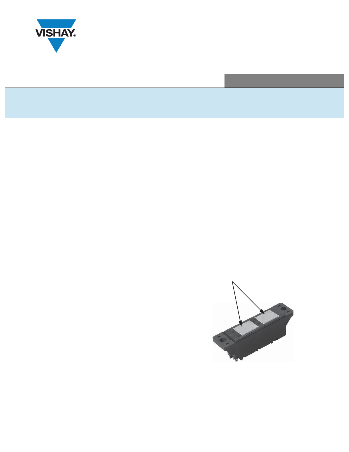
The AAP Generation VII modules are designed with an
exposed DBC Al2O3 substrate.
This is used to optimize the thermal behavior of the module.
To reduce the risk of damage during mounting, the ceramic
has been given additional mechanical ruggedness in the
form of two separate 15.8 mm by 21.1 mm (0.62" by 0.83")
pieces of DBC substrate, which can be seen in the photo
below.
APPLICATION NOTE
Before mounting, inspect the module to insure that the
contact surface of the bottom substrate is clean and free of
any lumps or bulges that could damage the device or
impede heat transfer across its surface.
Document Number: 95043
Revision: 17-Dec-08 1
Page 2

Application Note
Vishay Semiconductors
Mounting Instructions for
ADD-A-PAK Generation VII
Next, make a uniform coating on the heatsink mounting
surfaces and module substrate with a good quality thermal
compound. Screen printing of the compound is
recommended, as well as direct application through a roller
or spatula. The datasheet values for thermal resistance
assume a uniform layer of thermal compound with a
maximum thickness of 0.08 mm. The thermal conductivity of
the compound should be no less than 0.5 W/mK. Apply
uniform pressure on the package to force the compound to
spread over the entire contact area, and check the device
bottom surface to verify full and uniform coverage.
Bolt the module to the heatsink using the two fixing holes.
An even amount of torque should be applied for each
individual mounting screw. An M6 screw should be used
with lock washers. A torque wrench, which is accurate in the
specified range, must be used in mounting the module to
achieve optimum results. The first mounting screw should
be tightened to one third of the recommended torque; the
second screw should then be tightened to the same torque.
Full tightening of both the screws can then be completed by
applying the recommended torque (see data in bulletins).
Over-tightening the mounting screw may lead to
deformation of the package, which would hence increase
the thermal resistance and damage the semiconductors.
After a period of three hours, check the torque with a final
tightening in opposite sequence to allow the spread of the
compound.
Power terminals can be screwed to busbars and/or flexible
cables with eyelets.
We recommend the use of M5 screws with spring washers.
Users should consult published datasheets to determine the
optimal torque.
AAP Generation VII modules are designed to guarantee a
good and reliable contact even at 3 ± 10 % Nm on a busbar,
so there is no need to apply an especially high level of force
to obtain a good and reliable connection.
SOLDERING TO THE PCB
The signal terminal (gate and auxiliary cathode) pins of AAP
Gen VII modules based on thyristors can be soldered to the
PCB using hand iron or wave soldering processes.
The PCB should be designed with appropriate tolerances on
the hole diameters, and soldering must be done without
imposing any mechanical stress on the module pins (pulling
and tensioning the pins).
To prevent overheating of the device, the soldering time
should not exceed 8 s to 10 s at a temperature of 260 °C.
Alternatively, a fast-on cable connector can be used to
contact the signal pins.
APPLICATION NOTE
2 Revision: 17-Dec-08
Document Number: 95043
 Loading...