Vishay MMBZ27VDA-V Schematic [ru]

Small Signal Zener Diodes, Dual
Features
• Dual Silicon Planar Zener Diodes with
Common Anode configurations
• Dual package provides for Bidirectional or
separate unidirectional configurations
• The dual configurations protect two separate lines
with only one device
• Peak Power: 40 W at 1 ms (Bidirectional)
• For bidirectional operation, circuit connected to
pins 1 and 2. For unidirectional operation, circuit
connected to pins 1 and 3 or pins 2 and 3
• Lead (Pb)-free component
• Component in accordance to RoHS 2002/95/EC
and WEEE 2002/96/EC
e3
MMBZ27VDA-V
Vishay Semiconductors
MMBZ27VDA
3
12
Common Anode
20048
Marking:
MMBZ27VDA-V = TA7
Mechanical Data
Case: SOT-23 Plastic case
Weight: approx. 8.8 mg
Terminals: Solderable per MIL-STD-750,
method 2026
Packaging Codes/Options:
GS18/ 10 k per 13 " reel (8 mm tape), 10 k/box
GS08/ 3 k per 7 " reel (8 mm tape), 15 k/box
Absolute Maximum Ratings
T
= 25 °C, unless otherwise specified
amb
Parameter Test condition Symbol Value Unit
Peak power dissipation
Power dissipation
on FR-5 Board
Power dissipation
on Alumina Substrate
1)
Nonrepetitive current pulse per Figure 2 and derate above T
2)
FR-5 = 1.0 x 0.75 x 0.62 in.
3)
Alumina = 0.4 x 0.3 x 0.024 in., 99.5 % alumina.
1)
T
= 25 °C
2)
3)
amb
Derate above 25 °C
T
= 25 °C
amb
Derate above 25 °C
P
PK
P
tot
P
tot
= 25 °C per Figure 3.
amb
40 W
225
1.8
300
2.4
mW/°C
mW/°C
mW
mW
Thermal Characteristics
T
= 25 °C, unless otherwise specified
amb
Parameter Test condition Symbol Value Unit
Thermal resistance junction to ambiant air R
Operating and storage temperature range T
Document Number 81294
Rev. 1.0, 08-Mar-06
j
, T
thJA
stg
556 °C/W
- 55 to + 150 °C
www.vishay.com
1

MMBZ27VDA-V
Vishay Semiconductors
Electrical Characteristics
Partnumber Breakdown
1)
Voltage
VBR at I
T
V mA V nA A V mV/°C V mA
min max
MMBZ27VDA-V 25.65 28.35 1.0 22.0 80 1.0 38.0 30 1.1 200
Note:
1)
VBR measured at pulse test current IT at an ambient temperature of 25 °C
2)
Surge current waveform per Figure 2 and derate per Figure 3
Typical Characteristics
T
= 25 °C, unless otherwise specified
amb
Te st
Current
I
T
Working
Peak
Reverse
Voltage
V
RWM
Max.
Reverse
Leakage
Current
I
R
Max.
Reverse
Surge
Current
I
PP
Max. Reverse
Voltage
(Clamping
Voltage)
RSM
2)
VC at I
Max.
Temperature
Coefficient
at V
BR
Max. Forward
Voltage
V
F
at I
F
300
,POWER DISSIPATION (mW)
tot
P
18655
250
2
150
100
00
FR-5 BOARD
50
0
25
0
ALUMINA SUBSTRATE
7
5
5
0
T,
Temperature (°C)
1
00
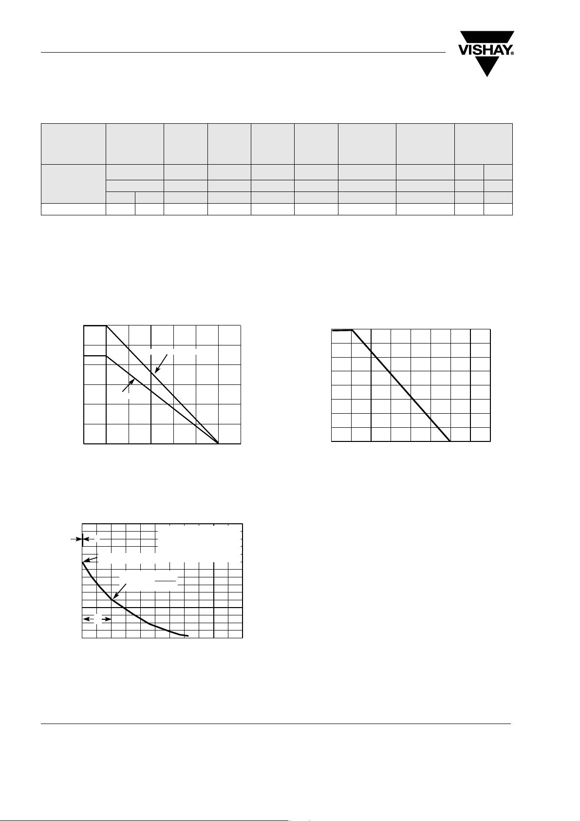
Figure 1. Steady State Power Derating Curve
t
r
100
Value (%)
Peak Value-I
Half Value-
50
Pulse width (tp) is defined
as that point where the
peak current decays to
50 % of I tr ≤ 10 µs
RSM
I
RSM
2
RSM
100
75
= 25 Z (°C)
A
50
2
5
power or current at T
Peak pulse derating in % of peak
18657
0
0
25
1
75
1
1
50
25
75
50
-
T
Ambient Temperature (°C)
A
100
125
200
175
15
0
Figure 3. Pulse Derating Curve
0
0
18656
www.vishay.com
2
tp
1
2
t, Time (ms)
Figure 2. Pulse Waveform
3
4
Document Number 81294
Rev. 1.0, 08-Mar-06
 Loading...